Tungsten diselenide
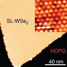 WSe2 monolayer on graphine (yellow) and its atomic image (inset)[1] | |
 | |
| Identifiers | |
|---|---|
3D model (JSmol) |
|
| ECHA InfoCard | 100.031.877 |
| EC Number | 235-078-7 |
PubChem CID |
|
| |
| |
| Properties | |
| WSe2 | |
| Molar mass | 341.76 g/mol |
| Appearance | grey to black solid |
| Odor | odorless |
| Density | 9.32 g/cm3[2] |
| Melting point | > 1200 °C |
| insoluble | |
| Band gap | ~1 eV (indirect, bulk)[3] ~1.7 eV (direct, monolayer)[4] |
| Structure | |
| hP6, space group P6 3/mmc, No 194[2] | |
a = 0.3297 nm, c = 1.2982 nm | |
| Trigonal prismatic (WIV) Pyramidal (Se2−) | |
| Hazards | |
| Main hazards | External MSDS |
Except where otherwise noted, data are given for materials in their standard state (at 25 °C [77 °F], 100 kPa). | |
| Infobox references | |
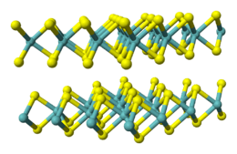
Tungsten diselenide is an inorganic compound with the formula WSe2.[5] The compound adopts a hexagonal crystalline structure similar to molybdenum disulfide. Every tungsten atom is covalently bonded to six selenium ligands in a trigonal prismatic coordination sphere while each selenium is bonded to three tungsten atoms in a pyramidal geometry. The tungsten–selenium bond has a length of 0.2526 nm, and the distance between selenium atoms is 0.334 nm.[6] Layers stack together via van der Waals interactions. WSe2 is a very stable semiconductor in the group-VI transition metal dichalcogenides.
Synthesis
Heating thin films of tungsten under pressure from gaseous selenium and high temperatures (>800 K) using the sputter deposition technique leads to the films crystallizing in hexagonal structures with the correct stoichiometric ratio.[7]
- W + 2 Se → WSe2
Potential applications
Transition metal dichalcogenides are semiconductors with potential applications in solar cells. Bulk WSe
2 has an optical band-gap of ~1.35 eV with a temperature dependence of −4.6×10⁻⁴ eV/K.[9] WSe
2 photoelectrodes are stable in both acidic and basic conditions, making them potentially useful in electrochemical solar cells.[10][11][12]
The properties of WSe
2 monolayers differ from those of the bulk state, as is typical for semiconductors. Mechanically exfoliated monolayers of WSe
2 are transparent photovoltaic materials with LED properties.[13] The resulting solar cells pass 95 percent of the incident light, with one tenth of the remaining five percent converted into electrical power.[14][15] The material can be changed from p-type to n-type by changing the voltage of an adjacent metal electrode from positive to negative, allowing devices made from it to have tunable bandgaps. As a result, it may enable LEDs of any color to be made from a single material.[16]
References
| Wikimedia Commons has media related to Tungsten diselenide. |
- ↑ Chiu, Ming-Hui; Zhang, Chendong; Shiu, Hung-Wei; Chuu, Chih-Piao; Chen, Chang-Hsiao; Chang, Chih-Yuan S.; Chen, Chia-Hao; Chou, Mei-Yin; Shih, Chih-Kang; Li, Lain-Jong (2015). "Determination of band alignment in the single-layer MoS2/WSe2 heterojunction". Nature Communications. 6: 7666. arXiv:1406.5137. Bibcode:2015NatCo...6E7666C. doi:10.1038/ncomms8666. PMC 4518320. PMID 26179885.
- 1 2 Agarwal, M. K.; Wani, P. A. (1979). "Growth conditions and crystal structure parameters of layer compounds in the series Mo1−xWxSe2". Materials Research Bulletin. 14 (6): 825–830. doi:10.1016/0025-5408(79)90144-2.
- ↑ Prakash, Abhijith; Appenzeller, Joerg (2017-02-28). "Bandgap Extraction and Device Analysis of Ionic Liquid Gated WSe2 Schottky Barrier Transistors". ACS Nano. 11 (2): 1626–1632. doi:10.1021/acsnano.6b07360. ISSN 1936-0851.
- ↑ Yun, Won Seok; Han, S. W.; Hong, Soon Cheol; Kim, In Gee; Lee, J. D. (2012). "Thickness and strain effects on electronic structures of transition metal dichalcogenides: 2H-MX2 semiconductors (M = Mo, W; X = S, Se, Te)". Physical Review B. 85 (3): 033305. Bibcode:2012PhRvB..85c3305Y. doi:10.1103/PhysRevB.85.033305.
- ↑ Holleman, Arnold Frederik; Wiberg, Egon (2001), Wiberg, Nils, ed., Inorganic Chemistry, translated by Eagleson, Mary; Brewer, William, San Diego/Berlin: Academic Press/De Gruyter, ISBN 0-12-352651-5
- ↑ Schutte, W.J.; De Boer, J.L.; Jellinek, F. (1986). "Crystal Structures of Tungsten Disulfide and Diselenide". Journal of Solid State Chemistry. 70 (2): 207–209. Bibcode:1987JSSCh..70..207S. doi:10.1016/0022-4596(87)90057-0.
- ↑ Pouzet, J.; Bernede, J.C.; Khellil, A.; Essaidi, H.; Benhida, S. (1992). "Preparation and characterization of tungsten diselenide thin films". Thin Solid Films. 208 (2): 252–259. Bibcode:1992TSF...208..252P. doi:10.1016/0040-6090(92)90652-R.
- ↑ Lin, Y. C.; Björkman, T. R.; Komsa, H. P.; Teng, P. Y.; Yeh, C. H.; Huang, F. S.; Lin, K. H.; Jadczak, J.; Huang, Y. S.; Chiu, P. W.; Krasheninnikov, A. V.; Suenaga, K. (2015). "Three-fold rotational defects in two-dimensional transition metal dichalcogenides". Nature Communications. 6: 6736. Bibcode:2015NatCo...6E6736L. doi:10.1038/ncomms7736. PMC 4396367. PMID 25832503.
- ↑ Upadhyayula, L.C.; Loferski, J.J.; Wold, A.; Giriat, W.; Kershaw, R. (1968). "Semiconducting Properties of Single Crystals of n- and p-Type Tungsten Diselenide (WSe2)". Journal of Applied Physics. 39 (10): 353–358. Bibcode:1968JAP....39.4736U. doi:10.1063/1.1655829.
- ↑ Gobrecht, J.; Gerischer, H.; Tributsch, H. (1978). "Electrochemical Solar Cell Based on the d-Band Semiconductor Tungsten-Diselenide". Berichte der Bunsengesellschaft für physikalische Chemie. 82 (12): 1331–1335. doi:10.1002/bbpc.19780821212.
- ↑ Xia, Fengnian; Wang, Han; Xiao, Di; Dubey, Madan; Ramasubramaniam, Ashwin (2014). "Two-dimensional material nanophotonics". Nature Photonics. 8 (12): 899. arXiv:1410.3882. Bibcode:2014NaPho...8..899X. doi:10.1038/nphoton.2014.271.
- ↑ Zhang, Xin; Qiao, Xiao-Fen; Shi, Wei; Wu, Jiang-Bin; Jiang, De-Sheng; Tan, Ping-Heng (2015). "Phonon and Raman scattering of two-dimensional transition metal dichalcogenides from monolayer, multilayer to bulk material". Chem. Soc. Rev. 44 (9): 2757. arXiv:1502.00701. doi:10.1039/C4CS00282B. PMID 25679474.
- ↑ Johnson, Dexter (11 March 2014). "Tungsten Diselenide Is New 2-D Optoelectronic Wonder Material". IEEE Spectrum. Retrieved 19 March 2014.
- ↑ "Tungsten diselenide shows potential for ultrathin, flexible, semi-transparent solar cells". Gizmag.com. 11 March 2014. Retrieved 17 August 2014.
- ↑ Florian Aigenr (10 March 2014). "Atomically thin solar cells" (Press release). Vienna University of Technology. Retrieved 18 August 2014.
- ↑ "One-molecule-thick material could lead to ultrathin, flexible solar cells and LEDs". Kurzweil Accelerating Intelligence newsletter. 11 March 2014.