Scanning thermal microscopy


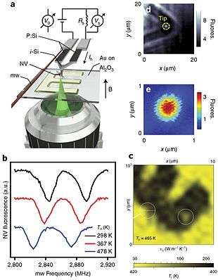
(a) Schematics of experimental setup. An electric current is applied to the arms of an AFM cantilever (phosphorus-doped Si, P:Si) and heats up the end section above the tip (intrinsic Si, i-Si). The bottom lens excites a diamond nanocrystal with a green laser light and collects photoluminescence (PL). The crystal hosts an N-V center and is attached to the AFM tip. A wire on the sample surface serves as the microwave source (mw). The temperature of the cantilever Th is determined from the applied current and voltage.
(b) Optically detected magnetic resonance spectra of the N-V center at three temperatures.
(c) Thermal conductivity image of a gold letter E on sapphire. White circles indicate features that do not correlate with the AFM topography. (d) PL image of the AFM cantilever end and tip where the diamond nanocrystal appears as the bright spot. (e) Zoomed PL image of the N-V center in d.[3]
Scanning thermal microscopy (SThM) is a type of scanning probe microscopy that maps the local temperature and thermal conductivity of an interface. The probe in a scanning thermal microscope is sensitive to local temperatures – providing a nano-scale thermometer. Thermal measurements at the nanometer scale are of both scientific and industrial interest.
Applications
SThM allows thermal measurements at the nano-scale. These measurements can include: temperature, thermal properties of materials, thermal conductivity, heat capacity, glass transition temperature, latent heat, enthalpy, etc. The applications include:
- Ultra large-scale integration (ULSI) lithography research and cellular diagnostics in biochemistry.[4][5][6][7]
- Detecting such parameters as phase changes in polymer blends.[8]
- Joule heating[9]
- Measuring material variations in semiconductor devices[10]
- Subsurface imaging[8][11]
- Near-field photo thermal micro-spectroscopy [12]
- Data storage[13][14]
- Calorimetry applications[4][5][15]
- Hot-spots in integrated circuits [16]
- Low temperature scanning thermal microscopy [17]
- Magnetic spectroscopy in combination with the ferromagnetic resonance realized in the SThM-FMR technique [18]
- Other applications[19]
History
Scanning thermal microscopy (SThM) was invented by Clayton C. Williams and H. Kumar Wickramasinghe in 1986.[20]
Technique
SThM requires the use of specialized probes. There are two types of thermal probes: Thermocouple probes where the probe temperature is monitored by a thermocouple junction at the probe tip and resistive or bolometer probes where the probe temperature is monitored by a thin-film resistor at probe tip. These probes are generally made from thin dielectric films on a silicon substrate and use a metal or semiconductor film bolometer to sense the tip temperature. Other approaches, using more involved micro machining methods, have also been reported.[21] In a bolometer probe the resistor is used as a local heater and the fractional change in probe resistance is used to detect the temperature and/or the thermal conductance of the sample.[15] When the tip is placed in contact with the sample, heat flows from the tip to sample. As the probe is scanned, the amount of heat flow changes. By monitoring the heat flow, one can create a thermal map of the sample, revealing spatial variations in thermal conductivity in a sample. Through a calibration process, the SThM can reveal the quantitative values of thermal conductivity.[22] Alternately the sample may be actively heated, for example a powered circuit, to visualize the distribution of temperatures on the sample.
Tip-sample heat transfer can include
- Solid-solid conduction. Probe tip to sample. This is the transfer mechanism which yields the thermal scan.
- Liquid-liquid conduction. When scanning in non-zero humidity, a liquid meniscus forms between the tip and sample. Conduction can occur through this liquid drop.
- Gas conduction. Heat can be transferred through the edges of the probe tip to the sample.
References
- ↑ Cui, Longji; Jeong, Wonho; Fernández-Hurtado, Víctor; Feist, Johannes; García-Vidal, Francisco J.; Cuevas, Juan Carlos; Meyhofer, Edgar; Reddy, Pramod (2017). "Study of radiative heat transfer in Ångström- and nanometre-sized gaps". Nature Communications. 8. Bibcode:2017NatCo...8.....C. doi:10.1038/ncomms14479. PMC 5330859. PMID 28198467.
- ↑ "TSPN". www.tspnano.com. Retrieved 2017-09-20.
- ↑ Laraoui, Abdelghani; Aycock-Rizzo, Halley; Gao, Yang; Lu, Xi; Riedo, Elisa; Meriles, Carlos A. (2015). "Imaging thermal conductivity with nanoscale resolution using a scanning spin probe". Nature Communications. 6: 8954. arXiv:1511.06916. Bibcode:2015NatCo...6E8954L. doi:10.1038/ncomms9954. PMC 4673876. PMID 26584676.
- 1 2 Li, M-H., Gianchandani, Y. B. (2003). "Applications of a low contact force polyimide shank bolometer probe for chemical and biological diagnostics". Sensors and Actuators A: Physical. 104 (3): 236–245. doi:10.1016/S0924-4247(03)00026-8.
- 1 2 Li, M-H.; et al. (2001). "Surface micromachined polyimide scanning thermocouple probes". IEEE/ASME Journal of Micro-electromechanical Systems. 10: 3–9. doi:10.1109/84.911085.
- ↑ Ocola, L. E.; et al. (1996). "Latent image formation: Nanoscale topography and calorimetric measurements in chemically amplified resists". Journal of Vacuum Science and Technology B. 14 (6): 3974–3979. Bibcode:1996JVSTB..14.3974O. doi:10.1116/1.588626.
- ↑ Basu, A. S.; et al. (2004). "Scanning thermal lithography: Maskless, submicron thermochemical patterning of photoresist by ultracompliant probes". Journal of Vacuum Science and Technology B. 22 (6): 3217–3220. Bibcode:2004JVSTB..22.3217B. doi:10.1116/1.1808732.
- 1 2 Hammiche, A.; et al. (1996). "Sub-surface imaging by scanning thermal microscopy". Meas. Sci. Technol. 7 (2): 142. Bibcode:1996MeScT...7..142H. doi:10.1088/0957-0233/7/2/004.
- ↑ Luo, K.; et al. (1996). "Nanofabrication of sensors on cantilever probe tips for scanning multiprobe microscopy". Appl. Phys. Lett. 68 (3): 325. Bibcode:1996ApPhL..68..325L. doi:10.1063/1.116074.
- ↑ Lai, J.; et al. (1995). "Thermal detection of device failure by atomic force microscopy". IEEE Electron Dev. Lett. 16 (7): 312. Bibcode:1995IEDL...16..312L. doi:10.1109/55.388718.
- ↑ Lee, J-H., Gianchandani, Y. B. Review of Scientific Instruments (2004). "High-resolution scanning thermal probe with servocontrolled interface circuit for microcalorimetry and other applications". Review of Scientific Instruments. 75 (5): 1222–1227. Bibcode:2004RScI...75.1222L. doi:10.1063/1.1711153.
- ↑ Hammiche, A.; et al. (1999). "Photothermal FT-IR Spectroscopy: A Step Towards FT-IR Microscopy at a Resolution Better Than the Diffraction Limit". Applied Spectroscopy. 53 (7): 810–815. Bibcode:1999ApSpe..53..810H. doi:10.1366/0003702991947379.
- ↑ Vettiger, P.; et al. (2000). "The “Millipede”—More than thousand tips for future AFM storage". IBM J. Res. Dev. 44 (3): 323–340. doi:10.1147/rd.443.0323.
- ↑ Lerchner, J.; et al. (2000). "Calorimetric detection of volatile organic compounds". Sensors and Actuators B: Chemical. 70: 57–66. doi:10.1016/S0925-4005(00)00554-2.
- 1 2 Lee, J-H. et al. International Workshop on Thermal Investigations of ICs and Systems (THERMINIC 2002), Madrid, Spain, October 2002, pp. 111–116.
- ↑ Hendarto, E.; et al. (2005). Proceedings 43rd Annual IEEE International Reliability Physics Symposium: 294–299
- ↑ J.Wu, M.Reading, D. Q. M. Craig (2008). "Application of Calorimetry, Sub-Ambient Atomic Force Microscopy and Dynamic Mechanical Analysis to the Study of Frozen Aqueous Trehalose Solutions". Pharmaceutical Research. 25 (6): 1396–1404. doi:10.1007/s11095-007-9530-y. PMID 18256792.
- ↑ R. Meckenstock; I. Barsukov; C. Bircan; A. Remhoff; D. Dietzel; D. Spoddig (2006). "Imaging of ferromagnetic resonance excitations in Permalloy nano structures on Si using scanning near-field thermal microscopy". J. Appl. Phys. 99 (8): 08C706. Bibcode:2006JAP....99hC706M. doi:10.1063/1.2171929.
- ↑ Majumdar A. Scanning thermal microscopy. Annu. Rev. Mater. Sci. (1999). "Scanning thermal microscopy". Annual Review of Materials Science. 29: 505. Bibcode:1999AnRMS..29..505M. doi:10.1146/annurev.matsci.29.1.505.
- ↑ Williams, C. C. and Wickramasinghe, H. K. (1986). "Scanning thermal profiler". Appl. Phys. Lett. 49 (23): 1587. Bibcode:1986ApPhL..49.1587W. doi:10.1063/1.97288.
- ↑ Gianchandani Y., Najafi, K. (1997). "A silicon micromachined scanning thermal profiler with integrated elements for sensing and actuation". IEEE Transactions on Electron Devices. 44 (11): 1857–1868. Bibcode:1997ITED...44.1857G. doi:10.1109/16.641353.
- ↑ Nasr Esfahani, Ehsan; Ma, Feiyue; Wang, Shanyu; Ou, Yun; Yang, Jihui; Li, Jiangyu (2017). "Quantitative nanoscale mapping of three-phase thermal conductivities in filled skutterudites via scanning thermal microscopy". National Science Review. 5: 59–69. doi:10.1093/nsr/nwx074.
External links
| Wikimedia Commons has media related to Scanning thermal microscopy. |