Optical proximity correction
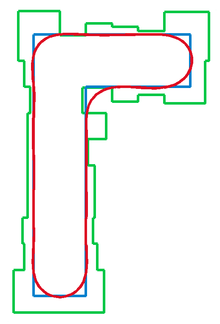
Optical proximity correction (OPC) is a photolithography enhancement technique commonly used to compensate for image errors due to diffraction or process effects. The need for OPC is seen mainly in the making of semiconductor devices and is due to the limitations of light to maintain the edge placement integrity of the original design, after processing, into the etched image on the silicon wafer. These projected images appear with irregularities such as line widths that are narrower or wider than designed, these are amenable to compensation by changing the pattern on the photomask used for imaging. Other distortions such as rounded corners are driven by the resolution of the optical imaging tool and are harder to compensate for. Such distortions, if not corrected for, may significantly alter the electrical properties of what was being fabricated. Optical proximity correction corrects these errors by moving edges or adding extra polygons to the pattern written on the photomask. This may be driven by pre-computed look-up tables based on width and spacing between features (known as rule based OPC) or by using compact models to dynamically simulate the final pattern and thereby drive the movement of edges, typically broken into sections, to find the best solution, (this is known as model based OPC). The objective is to reproduce on the semiconductor wafer, as well as possible, the original layout drawn by the designer.
The two most visible benefits of OPC are correcting linewidth differences seen between features in regions of different density (e.g., center vs. edge of an array, or nested vs. isolated lines), and line end shortening (e.g., gate overlap on field oxide). For the former case, this may be used together with resolution enhancement technologies such as scattering bars (sub-resolution lines placed adjacent to resolvable lines) together with linewidth adjustments. For the latter case, "dog-ear" (serif or hammerhead) features may be generated at the line end in the design. OPC has a cost impact on photomask fabrication whereby the mask write time is related to the complexity of the mask and data-files and similarly mask inspection for defects takes longer as the finer edge control requires a smaller spot size.
Impact of resolution: the k1 factor
The conventional diffraction-limited resolution is given by the Rayleigh criterion as where is the numerical aperture and is the wavelength of the illumination source. It is often common to compare the critical feature width to this value, by defining a parameter, such that feature width equals Nested features with benefit less from OPC than isolated features of the same size. The reason is the spatial frequency spectrum of nested features contains fewer components than isolated features. As the feature pitch decreases, more components are truncated by the numerical aperture, resulting in greater difficulty to affect the pattern in the desired fashion.


Impact of illumination and spatial coherence
The degree of coherence of the illumination source is determined by the ratio of its angular extent to the numerical aperture. This ratio is often called the partial coherence factor, or .[1] It also affects the pattern quality and hence the application of OPC. The coherence distance in the image plane is given roughly by [2] Two image points separated by more than this distance will effectively be uncorrelated, allowing a simpler OPC application. This distance is in fact close to the Rayleigh criterion for values of close to 1.


A related point is that the use of OPC does not change the illumination requirement. If off-axis illumination is required, OPC cannot be used to switch to on-axis illumination, because for on-axis illumination, imaging information is scattered outside the final aperture when off-axis illumination is needed, preventing any imaging.
Impact of aberrations
Aberrations in optical projection systems deform wavefronts, or the spectrum or spread of illumination angles, which can affect the depth of focus. While the use of OPC can offer significant benefits to depth of focus, aberrations can more than offset these benefits.[3] Good depth of focus requires diffracted light traveling at comparable angles with the optical axis, and this requires the appropriate illumination angle.[4] Assuming the correct illumination angle, OPC can direct more diffracted light along the right angles for a given pitch, but without the correct illumination angle, such angles will not even arise.
Impact of multiple exposure
As the factor has been steadily shrinking over the past technology generations, the anticipated requirement of moving to multiple exposure to generate circuit patterns becomes more real. This approach will affect the application of OPC, as one will need to take into account the sum of the image intensities from each exposure. This is the case for the complementary photomask technique,[5] where the images of an alternating-aperture phase-shifting mask and a conventional binary mask are added together.

Impact of multiple-etch patterning
In contrast to multiple exposure of the same photoresist film, multiple layer patterning entails repeated photoresist coating, deposition, and etching to pattern the same device layer. This gives an opportunity to use looser design rules to pattern the same layer. Depending on the lithography tool used to image at these looser design rules, the OPC will be different. Multiple-etch patterning may become a popular technique for future technology generations. A specific form of multiple-etch patterning, using sidewall sacrificial features, is currently the only demonstrated way of systematically patterning features less than 10 nm.[6] The minimum half-pitch corresponds to the deposited thickness of the sacrificial feature.
OPC application today
Today, OPC is rarely practiced without the use of commercial packages from electronic design automation (EDA) vendors. Advances in algorithms, modeling techniques and the use of large compute farms has enabled the most critical patterning layers to be corrected overnight, starting from the 130 nm design rules (when model based OPC was first used) [7] down to the most advanced designs of today using 32 nm design rules. The number of layers requiring sophisticated OPC has increased with advanced nodes, as previously non-critical layers now require compensation.
The use of OPC is not restricted to the low features which are commonly encountered today, but can be applied to any desired image correction scheme which can be modeled accurately. For example, proximity effect correction in electron beam lithography is included as an automated capability on commercial electron-beam lithography tools. Since many non-lithographic processes exhibit their own proximity effects, e.g., chemical-mechanical polishing or plasma etching, these effects can be mixed in with the original OPC.
Subresolution assist features (SRAFs)
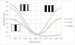
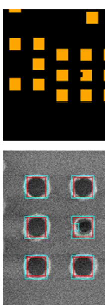
Subresolution assist features (SRAFs) are features which are separated from targeted features but assist in their printing, while not being printed themselves. Printing SRAFs are a critical yield detractor and require additional OPC models to determine and remove SRAFs where undesirable printing may occur.[8] SRAFs have more pronounced effects on the diffraction spectrum than targeted feature resizing and/or attachments. The requirement to not print constrains their use with low doses only. Hence their main application is to improve depth of focus for isolated features (dense features do not leave enough room for SRAF placement). Since SRAFs redistribute energy toward higher spatial frequencies or diffraction orders, the depth of focus is more dependent on the illumination angle (center of spectrum of spatial frequencies or diffraction orders) as well as the pitch (separation of spatial frequences or diffraction orders). In particular, different SRAFs (position, shape, size) could result in different illumination specifications.[9][10] In fact, certain pitches forbid the use of SRAFs for specific illumination angles.[11] Since the pitch is usually predetermined, some illumination angles must be avoided even with the use of SRAF OPC.
See also
References
- ↑ K. Ronse et al., J. Vac. Sci. and Tech. B, vol. 12, pp. 589-600 (1994).
- ↑ B. E. A. Saleh and M. C. Teich, Fundamentals of Photonics, pp. 364-5 (Wiley, 1991).
- ↑ A. Kroyan, M. D. Levenson, and F. K. Tittel, Proc. SPIE 3334, 832 (1998).
- ↑ H. J. Levinson, Principles of Lithography (2nd ed.), 2005, pp. 274-276.
- ↑ M. E. Kling et al., Proc. SPIE vol. 3679, pp.10-17 (1999)
- ↑ Y-K Choi et al., J. Phys. Chem. B, vol. 107, pp. 3340-3343 (2003).
- ↑ J. Stirniman and M. Rieger. Fast proximity correction with zone sampling. Proc. SPIE Vol 2197, pp 294-301, (1994).
- ↑ K. Kohli et al., Proc. SPIE 10147, 101470O (2017)
- ↑ L. Pang et al., Proc. SPIE 7520, 75200X (2009).
- ↑ S. Nagahara et al., Proc. SPIE 7640, 76401H (2010).
- ↑ X. Shi et al., Proc. SPIE 4689, 985 (2002).