Gary Patton
Dr. Gary Patton is an American technologist and business executive. He is currently the Chief Technology Officer and Senior Vice President of Worldwide Research and Development (R&D) at GlobalFoundries. He spent his early career at IBM, and he was appointed CTO of GlobalFoundries in 2015.
Early life and education
Dr. Patton was born and raised in Glendale, CA. He received his B.S. degree in electrical engineering from UCLA, where he graduated Summa Cum Laude and Phi Beta Kappa, and his M.S. and Ph.D. degrees in electrical engineering from Stanford University. His Ph.D. work was on the physics of polycrystalline silicon emitters for bipolar transistors.[1][2] Dr. Patton was the first in his family to attend college.
Career
1986–2015: IBM
Dr. Patton was with IBM for almost 30 years, starting in 1986 at IBM's T.J. Watson Research Center. He held management and executive positions in research, technology and product development, manufacturing, and business unit management in IBM's Research, Microelectronics, and Storage Technology Divisions. He was selected to be a member of IBM Corporate's Growth & Transformation Team (G&TT), a group consisting of approximately 300 of the top IBM executives chartered with driving growth and transformation initiatives across the company.
During the last eight years of his career at IBM, Patton was Vice President of IBM's Semiconductor Research and Development Center (SRDC), where he was responsible for IBM’s semiconductor R&D roadmap, operations, execution, and technology development alliances.[3][4] As the head of IBM’s SRDC, he led the teams responsible for the development of multiple generations of leading-edge process technologies (45 nm through 7 nm technologies).[5][6][7][8] These technologies powered next-generation IBM servers and a wide range of consumer products, and incorporated major technology innovations such as Silicon-On-Insulator, advanced strain engineering, embedded DRAM memory solutions, high-k/metal gate[9] and FinFET technologies. Dr. Patton drove the introduction of high performance embedded DRAM memory into IBM microprocessors at 45 nm. By addressing microprocessor memory bandwidth issues, this new technology improved microprocessor performance in multi-core designs, and accelerated the movement of graphics in gaming, networking, and other image intensive, multi-media applications.[10][11] He also led the development of the IBM Alliance’s 32/28 nm high-k.metal gate technologies currently used today in a wide range of consumer and industrial applications.[6][8][12] This innovation reduced transistor power requirements while simultaneously delivering improved circuit speed.
During this time, Dr. Patton also led IBM’s advanced technology R&D efforts at the State University of New York (SUNY) Polytechnic Institute, pioneering many innovations in collaboration with IBM’s research partners. These innovations included the development of 14 nm FinFET technology, which has since been commercialized, and the semiconductor industry’s first 7 nm test chips with functioning transistors.[13] Among the novel processes and techniques pioneered at 7 nm were a number of industry-first innovations, most notably Silicon Germanium (SiGe) channel FinFET transistors and the use of Extreme Ultraviolet (EUV) lithography.
Dr. Patton was involved with IBM’s technology development alliances from its very beginning in the early 1990’s. In 1992, he led the IBM-Siemens-Toshiba 64Mb DRAM technology development team and delivered this technology into manufacturing. He assumed senior management positions in manufacturing engineering and production operations in IBM's Advanced Semiconductor Technology Center, the facility where IBM's technology development alliance work took place. He then served as the Executive Assistant to the Senior Vice President of IBM’s Technology Group. This led to Dr. Patton's executive appointment in 1999 as the Director of IBM Microelectronics' Wireless Business Unit. In 2002, he moved to IBM's Storage Technology Division, where he was the Vice President of research and development of magnetic heads and media for IBM's Hard Disk Drive products. IBM sold this business to Hitachi in 2003 and it was merged with Hitachi's Hard Disk Drive business to become Hitachi Global Storage Technology (HGST). He was Vice President & General Manager for HGST's Head & Media Business Unit, as well as the General Manager for HGST's San Jose, CA site. He returned to IBM in 2005 as Vice President of Technology Development in IBM Microelectronics Divisions' SRDC. He was asked to lead the SRDC in 2007. He held this position for eight years, until GlobalFoundries' acquisition of IBM's Microelectronics Division.
During his career at IBM, Patton’s pioneering work on SiGe Heterojunction Bipolar Transistors (HBT) created the foundation for today’s SiGe HBT BiCMOS technologies which are used in a wide range of wireless communication devices (e.g., cell phones, PDAs, wireless LANs, GPS devices). In the late 1980's, he and a small team of researchers at IBM’s T.J. Watson Research Center demonstrated the first working SiGe heterojunction transistor and established a world record for silicon transistor performance, tripling the previous record.[14][15][16][17] They also developed the first manufacturable approach for making a high volume SiGe BiCMOS technology. Later, as the head of IBM Microelectronics' wireless business unit, which was effectively a start-up business at that time, Patton drove industry adoption of IBM’s SiGe BiCMOS technology and other radio frequency (RF), analog, and mixed signal technology offerings. Today, most mobile devices contain several chips manufactured using these technologies.
2015–present: GlobalFoundries

Patton is presently GlobalFoundries’ CTO and responsible for the company’s semiconductor technology research and development roadmap, operations, and execution.[18][19][20] He joined GlobalFoundries in July 2015 with GlobalFoundries' acquisition of IBM's Microelectronics Division.
Dr. Patton has co-authored over 70 technical papers and given numerous keynote and panel talks at major industry forums (e.g. IEEE Transactions on Electron Devices and Electron Device Letters, International Electron Device Meetings (IEDM), Symposium on VLSI Technology, SEMI ISS and SMC Conferences, Design Automation Conference (DAC), Confab, Common Platform Technology Forum, GlobalFoundries' Technology Conference). He has served on the IEEE Nishizawa Medal and IEEE Grove Field Award Committees, the Semiconductor Research Corporation (SRC) Board, the Confab Advisory Board, and the Executive Advisory Committee of SEMI's Semiconductor Components, Instruments, and Subsystems (SCIS) initiative.[21] He also served as the Technical Program Chairman for the Bipolar Circuits and Technology Conference (BCTM).
Awards and honors
Dr. Patton was elected a Fellow of the Institute of Electrical and Electronics Engineers (IEEE) in 2010 for his contribution to silicon germanium heterojunction bipolar transistors.[22][23] Dr. Patton’s pioneering work on SiGe HBTs was recognized at the 2004 International Electron Device Meetings 50th Anniversary event as the key innovation of 1987. He received an Outstanding Technology Achievement Award from IBM in 1989 for this work.
During his career at IBM, he received Outstanding Technical Achievement, Research Division, Microelectronics Division, and General Manager's Excellence Awards for his work.
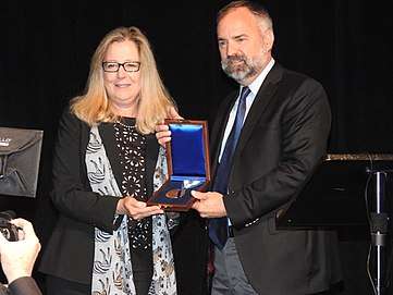
In 2016, he was inducted into VLSI Research's Chip Making Industry Hall of Fame for decades of technology vision and leadership at IBM and now GlobalFoundries.[24]
In 2017, Dr. Patton received the IEEE Frederik Philips Award, for outstanding accomplishments in the management of research and development resulting in effective innovation in the electrical and electronics industry.[25][26]
References
- ↑ G.L. Patton, J.C. Bravman, J.D. Plummer (November 1986). "Physics, Technology, and Modeling of Polysilicon Emitter Contacts for VLSI Bipolar Transistors". IEEE Trans. Electron Devices. ED-33: 1754–1768.
- ↑ G.L. Patton, J.C. Bravman, J.D. Plummer (December 1985). "Impact of Processing Parameters on Base Current in Polysilicon-Contacted Bipolar Transitors". IEDM Tech. Dig. 1985: 30–33.
- ↑ Patton, Gary (2008). "VLSI Research Interview: What Math & Science Have Done For Me". Chip History Center.
- ↑ Patton, Gary (2013). "Collaboration as a Way Forward in Semiconductor Technology". IESA Vision Summit, Bangalore, India.
- ↑ "AMD and IBM Detail Early Results Using Immersion and Ultra Low-K in 45nm Chips". IBM. December 12, 2006.
- 1 2 "IBM-Led Chip Alliance Delivers Major Semiconductor Performance Leap, Power Savings Using Innovative "High-K/Metal Gate" Material". IBM. April 14, 2008.
- ↑ "IBM Develops Computational Scaling Solution for Next Generation "22nm" Semiconductors". IBM. September 17, 2008.
- 1 2 "BM Technology Alliance Announces Availability of Advanced 28-Nanometer, Low-Power Semiconductor Technology". IBM. April 16, 2009.
- ↑ M.Khare, G.L. Patton (January 2008). "High-k/Metal Gate Technology". IET & GSA Intl Semiconductor Forum. 2008: 34–35.
- ↑ "IBM Unveils World's Fastest On-Chip Dynamic Memory Technology". IBM. February 14, 2007.
- ↑ "IBM Announces Industry's Densest, Fastest On-Chip Dynamic Memory in 32-Nanometer, Silicon-on-Insulator Technology". IBM. September 18, 2009.
- ↑ Patton, Gary (April 29, 2008). "VLSI Research Interview: IBM's 32nm Hi-K Chip Technology: An interview with Gary Patton". weSRCH.
- ↑ "IBM Research Alliance Produces Industry's First 7nm Node Test Chips". IBM. July 9, 2015.
- ↑ G.L. Patton, J.H. Comfort, B.S. Meyerson, E.F. Crabbe, G.J. Scilla, E. deFresart, J.M.C. Stork, J.Y.-C. Sun, D.L. Harame, J.N. Burghartz (June 1990). "63-75 GHz fT-SiGe-Base Heterojunction Bipolar Technology". 1989 Symp. on VLSI Technol. Dig. 1990: 49–50.
- ↑ S.S. Iyer, G.L. Patton, S.L. Delage, S. Tiwari, J.M.C. Stork (December 1987). "Silicon-Germanium Base Heterojunction Bipolar Transistors by Molecular Beam Epitaxy". IEDM Tech. Dig: 874–876.
- ↑ G.L. Patton, J.H. Comfort, B.S. Meyerson, E.F. Crabbe, G.J. Scilla, E. deFresart, J.M.C. Stork, J.Y.-C. Sun, D.L. Harame, J.N. Burghartz (April 1990). "75 GHz SiGe-Base Heterojunction Bipolar Transistors". IEEE Electron Device Letters. 11.
- ↑ S.S. Iyer, G.L. Patton, S.L. Delage, S. Tiwari, J.M.C. Stork (October 1987). "Silicon-Germanium Base Heterojunction Bipolar Transistor by MBE". Proc. 2nd Intl Sump. on Si MBE.
- ↑ Patton, Gary (October 15, 2015). "VLSI Research Interview: FinFET vs FDSOI in the jump to 7nm". weSRCH.
- ↑ "GLOBALFOUNDRIES on Track to Deliver Leading-Performance 7nm FinFET Technology". GLOBALFOUNDRIES. June 13, 2017.
- ↑ "A 7nm CMOS Technology Platform for Mobile and High-Performance Compute Applications". IEEE International Electron Device Meetings. December 13, 2017.
- ↑ "SEMI SCIS Special Interest Group".
- ↑ "IEEE Fellows Class of 2010" (PDF).
- ↑ "IEEE Fellows Directory".
- ↑ "Chip Making Industry Hall of Fame". The Chip History Center - The Virtual Museum of Semiconductors. 2016.
- ↑ "IEEE Frederik Philips Award recipients".
- ↑ "IEEE R1 Highlights".