Bismuth telluride
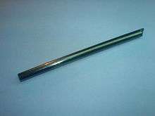 Single crystal of bismuth telluride | |
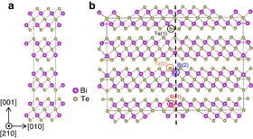 Atomic structure: ideal (l) and with a twin defect (r) | |
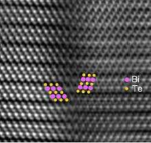 Electron micrograph of twinned bismuth telluride | |
| Identifiers | |
|---|---|
3D model (JSmol) |
|
| ChemSpider | |
| ECHA InfoCard | 100.013.760 |
| EC Number | 215-135-2 |
PubChem CID |
|
| |
| |
| Properties | |
| Bi2Te3 | |
| Molar mass | 800.76 g/mol[1] |
| Appearance | grey powder |
| Density | 7.74 g/cm3[1] |
| Melting point | 580 °C (1,076 °F; 853 K)[1] |
| insoluble[1] | |
| Solubility in ethanol | soluble[1] |
| Structure | |
| Trigonal, hR15 | |
| R3m, No. 166[2] | |
a = 0.4395 nm, c = 3.044 nm | |
Formula units (Z) |
3 |
| Hazards | |
| Safety data sheet | Sigma-Aldrich |
| NFPA 704 | |
| Flash point | noncombustible [3] |
| US health exposure limits (NIOSH): | |
PEL (Permissible) |
TWA 15 mg/m3 (total) TWA 5 mg/m3 (resp) (pure) none (doped with selenium sulfide) [3] |
REL (Recommended) |
TWA 10 mg/m3 (total) TWA 5 mg/m3 (resp) (pure) TWA 5 mg/m3 (doped with selenium sulfide)[3] |
IDLH (Immediate danger) |
N.D. (pure and doped)[3] |
Except where otherwise noted, data are given for materials in their standard state (at 25 °C [77 °F], 100 kPa). | |
| Infobox references | |

Bismuth telluride (Bi2Te3) is a gray powder that is a compound of bismuth and tellurium also known as bismuth(III) telluride. It is a semiconductor, which, when alloyed with antimony or selenium, is an efficient thermoelectric material for refrigeration or portable power generation. Bi2Te3 is a topological insulator, and thus exhibits thickness-dependent physical properties.
Properties as a thermoelectric material
Bismuth telluride is a narrow-gap layered semiconductor with a trigonal unit cell. The valence and conduction band structure can be described as a many-ellipsoidal model with 6 constant-energy ellipsoids that are centered on the reflection planes.[4] Bi2Te3 cleaves easily along the trigonal axis due to Van der Waals bonding between neighboring tellurium atoms. Due to this, bismuth-telluride-based materials used for power generation or cooling applications must be polycrystalline. Furthermore, the Seebeck coefficient of bulk Bi2Te3 becomes compensated around room temperature, forcing the materials used in power-generation devices to be an alloy of bismuth, antimony, tellurium, and selenium.[5]
Recently, researchers have attempted to improve the efficiency of Bi2Te3-based materials by creating structures where one or more dimensions are reduced, such as nanowires or thin films. In one such instance n-type bismuth telluride was shown to have an improved Seebeck coefficient (voltage per unit temperature difference) of −287 μV/K at 54 °C,[6] However, one must realize that Seebeck coefficient and electrical conductivity have a tradeoff: a higher Seebeck coefficient results in decreased carrier concentration and decreased electrical conductivity.[7]
In another case, researchers report that bismuth telluride has high electrical conductivity of 1.1×10⁵ S·m/m2 with its very low lattice thermal conductivity of 1.20 W/(m·K), similar to ordinary glass.[8]
Properties as a topological insulator
Bismuth telluride is a well-studied topological insulator. Its physical properties have been shown to change at highly reduced thicknesses, when its conducting surface states are exposed and isolated. These thin samples are obtained through either epitaxy or mechanical exfoliation.
Epitaxial growth methods such as molecular beam epitaxy and metal organic chemical vapor deposition are common methods of obtaining thin Bi2Te3 samples. The stoichiometry of samples obtained through such techniques can vary greatly between experiments, so Raman spectroscopy is often used to determine relative purity. However, thin Bi2Te3 samples are resistant to Raman spectroscopy due to their low melting point and poor heat dispersion.[9]
The crystalline structure of Bi2Te3 allows for mechanical exfoliation of thin samples by cleaving along the trigonal axis. This process is significantly lower in yield than epitaxial growth, but produces samples without defects or impurities. Similar to extracting graphene from bulk graphite samples, this is done by applying and removing adhesive tape from successively thinner samples. This procedure has been used to obtain Bi2Te3 flakes with a thickness of 1 nm.[10] However, this process can leave significant amounts of adhesive residue on a standard Si/SiO2 substrate, which in turn obscure atomic force microscopy measurements and inhibit the placement of contacts on the substrate for purposes of testing. Common cleaning techniques such as oxygen plasma, boiling acetone and isopropyl alcohol are ineffective in removing residue..[11]
Occurrence
The mineral form of Bi2Te3 is tellurobismuthite which is moderately rare. There are many natural bismuth tellurides of different stoichiometry, as well as compounds of the Bi-Te-S-(Se) system, like Bi2Te2S (tetradymite).
Preparation
Bismuth telluride is prepared by sealing a sample of bismuth and tellurium metal in a quartz tube under vacuum (critical, as an unsealed or leaking sample may explode in a furnace) and heating it to 800 °C in a muffle furnace.
See also
References
- 1 2 3 4 5 Haynes, William M., ed. (2011). CRC Handbook of Chemistry and Physics (92nd ed.). Boca Raton, FL: CRC Press. p. 4.52. ISBN 1439855110.
- ↑ Feutelais, Y.; Legendre, B.; Rodier, N.; Agafonov, V. (1993). "A study of the phases in the bismuth – tellurium system". Materials Research Bulletin. 28 (6): 591. doi:10.1016/0025-5408(93)90055-I.
- 1 2 3 4 "NIOSH Pocket Guide to Chemical Hazards #0056". National Institute for Occupational Safety and Health (NIOSH).
- ↑ Caywood, L. P.; Miller, G. (1970). "Anisotropy of the constant energy surfaces in p-type Bi2Te3 and Bi2Se3 from galvanomagnetic coefficients". Phys. Rev. B. 2 (8): 3209. Bibcode:1970PhRvB...2.3209C. doi:10.1103/PhysRevB.2.3209.
- ↑ Satterthwaite, C. B.; Ure, R. (1957). "Electrical and Thermal Properties of Bi2Te3". Phys. Rev. 108 (5): 1164. Bibcode:1957PhRv..108.1164S. doi:10.1103/PhysRev.108.1164.
- ↑ Tan, J. (2005). "Thermoelectric properties of bismuth telluride thin films deposited by radio frequency magnetron sputtering". Proceedings of SPIE. Proceedings of the SPIE. Smart Sensors, Actuators, and MEMS II. 5836. p. 711. Bibcode:2005SPIE.5836..711T. doi:10.1117/12.609819.
- ↑ Goldsmid, H. J.; Sheard, A. R. & Wright, D. A. (1958). "The performance of bismuth telluride thermojunctions". Br. J. Appl. Phys. 9 (9): 365. Bibcode:1958BJAP....9..365G. doi:10.1088/0508-3443/9/9/306.
- ↑ Takeiishi, M.; et al. "Thermal conductivity measurements of Bismuth Telluride thin films by using the 3 Omega method" (PDF). The 27th Japan Symposium on Thermophysical Properties, 2006, Kyoto. Archived from the original (PDF) on 2007-06-28. Retrieved 2009-06-06.
- ↑ Teweldebrhan, D.; Goyal, V.; Balandin, A. A, (2010). "From Graphene to Bismuth Telluride: Mechanical Exfoliation of Quasi-2D Crystals for Applications in Thermoelectrics and Topological Insulators". Nano Letters. 10 (12): 1209. Bibcode:2010NanoL..10.1209T. doi:10.1021/nl903590b.
- ↑ Teweldebrhan, D.; Goyal, V.; Rahman, M.; Balandin, A. A. (2010). ""Graphene-like" exfoliation of atomically-thin bismuth telluride films". Appl. Phys. Let. ECS Transactions. 96: 053107. doi:10.1149/1.3485611.
- ↑ Childresa, I.; Tiana, J.; Miotkowskia, I.; Chen, Y. (2011). "AFM and Raman studies of topological insulator materials subject to argon plasma etching". Philosophical Magazine. 93 (6): 681–689. doi:10.1149/1.3485611.
External links
| Wikimedia Commons has media related to Bismuth telluride. |