PCI Express
PCI Express (Peripheral Component Interconnect Express), officially abbreviated as PCIe or PCI-e,[1] is a high-speed serial computer expansion bus standard, designed to replace the older PCI, PCI-X and AGP bus standards. It is the common motherboard interface for personal computers' graphics cards, hard drives, SSDs, Wi-Fi and Ethernet hardware connections.[2] PCIe has numerous improvements over the older standards, including higher maximum system bus throughput, lower I/O pin count and smaller physical footprint, better performance scaling for bus devices, a more detailed error detection and reporting mechanism (Advanced Error Reporting, AER[3]), and native hot-swap functionality. More recent revisions of the PCIe standard provide hardware support for I/O virtualization.
| Year created | 2003 |
|---|---|
| Created by | |
| Supersedes | |
| Width in bits | 1 per lane; 1–16 bonded lanes |
| No. of devices | One device each on each endpoint of each connection. PCI Express switches can create multiple endpoints out of one endpoint to allow sharing one endpoint with multiple devices. |
| Speed | For single-lane (x1) and 16-lane (x16) links, in each direction (GT/s == Gbit/s encoded bit rate):
|
| Style | Serial |
| Hotplugging interface | Yes, if ExpressCard, Mobile PCI Express Module, XQD card or Thunderbolt |
| External interface | Yes, with PCI Express OCuLink and External Cabling, such as Thunderbolt |
| Website | pcisig |
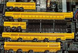
- PCI Express x4
- PCI Express x16
- PCI Express x1
- PCI Express x16
- Conventional PCI (32-bit, 5 V)
Defined by its number of lanes,[4] the PCI Express electrical interface is also used in a variety of other standards, most notably the laptop expansion card interface ExpressCard and computer storage interfaces SATA Express, U.2 (SFF-8639) and M.2.
Format specifications are maintained and developed by the PCI-SIG (PCI Special Interest Group), a group of more than 900 companies that also maintain the conventional PCI specifications.
Architecture
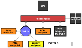
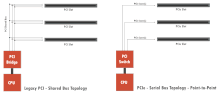
white "junction boxes" represent PCI Express device downstream ports, while the gray ones represent upstream ports.[5]:7
Conceptually, the PCI Express bus is a high-speed serial replacement of the older PCI/PCI-X bus.[6] One of the key differences between the PCI Express bus and the older PCI is the bus topology; PCI uses a shared parallel bus architecture, in which the PCI host and all devices share a common set of address, data and control lines. In contrast, PCI Express is based on point-to-point topology, with separate serial links connecting every device to the root complex (host). Because of its shared bus topology, access to the older PCI bus is arbitrated (in the case of multiple masters), and limited to one master at a time, in a single direction. Furthermore, the older PCI clocking scheme limits the bus clock to the slowest peripheral on the bus (regardless of the devices involved in the bus transaction). In contrast, a PCI Express bus link supports full-duplex communication between any two endpoints, with no inherent limitation on concurrent access across multiple endpoints.
In terms of bus protocol, PCI Express communication is encapsulated in packets. The work of packetizing and de-packetizing data and status-message traffic is handled by the transaction layer of the PCI Express port (described later). Radical differences in electrical signaling and bus protocol require the use of a different mechanical form factor and expansion connectors (and thus, new motherboards and new adapter boards); PCI slots and PCI Express slots are not interchangeable. At the software level, PCI Express preserves backward compatibility with PCI; legacy PCI system software can detect and configure newer PCI Express devices without explicit support for the PCI Express standard, though new PCI Express features are inaccessible.
The PCI Express link between two devices can vary in size from one to 32 lanes. In a multi-lane link, the packet data is striped across lanes, and peak data throughput scales with the overall link width. The lane count is automatically negotiated during device initialization, and can be restricted by either endpoint. For example, a single-lane PCI Express (x1) card can be inserted into a multi-lane slot (x4, x8, etc.), and the initialization cycle auto-negotiates the highest mutually supported lane count. The link can dynamically down-configure itself to use fewer lanes, providing a failure tolerance in case bad or unreliable lanes are present. The PCI Express standard defines link widths of x1, x4, x8, x12, x16, and x32.[5]:4,5[7] This allows the PCI Express bus to serve both cost-sensitive applications where high throughput is not needed, and performance-critical applications such as 3D graphics, networking (10 Gigabit Ethernet or multiport Gigabit Ethernet), and enterprise storage (SAS or Fibre Channel). Slots and connectors are only defined for a subset of these widths, with link widths in between using the next larger physical slot size.
As a point of reference, a PCI-X (133 MHz 64-bit) device and a PCI Express 1.0 device using four lanes (x4) have roughly the same peak single-direction transfer rate of 1064 MB/s. The PCI Express bus has the potential to perform better than the PCI-X bus in cases where multiple devices are transferring data simultaneously, or if communication with the PCI Express peripheral is bidirectional.
Interconnect
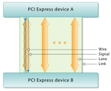
PCI Express devices communicate via a logical connection called an interconnect[8] or link. A link is a point-to-point communication channel between two PCI Express ports allowing both of them to send and receive ordinary PCI requests (configuration, I/O or memory read/write) and interrupts (INTx, MSI or MSI-X). At the physical level, a link is composed of one or more lanes.[8] Low-speed peripherals (such as an 802.11 Wi-Fi card) use a single-lane (x1) link, while a graphics adapter typically uses a much wider and therefore faster 16-lane (x16) link.
Lane
A lane is composed of two differential signaling pairs, with one pair for receiving data and the other for transmitting. Thus, each lane is composed of four wires or signal traces. Conceptually, each lane is used as a full-duplex byte stream, transporting data packets in eight-bit "byte" format simultaneously in both directions between endpoints of a link.[9] Physical PCI Express links may contain from 1 to 16 lanes, more precisely 1, 4, 8 or 16 lanes.[10][5]:4,5[8] Lane counts are written with an "x" prefix (for example, "x8" represents an eight-lane card or slot), with x16 being the largest size in common use.[11] Lane sizes are also referred to via the terms "width" or "by" e.g., an eight-lane slot could be referred to as a "by 8" or as "8 lanes wide."
For mechanical card sizes, see below.
Serial bus
The bonded serial bus architecture was chosen over the traditional parallel bus because of inherent limitations of the latter, including half-duplex operation, excess signal count, and inherently lower bandwidth due to timing skew. Timing skew results from separate electrical signals within a parallel interface traveling through conductors of different lengths, on potentially different printed circuit board (PCB) layers, and at possibly different signal velocities. Despite being transmitted simultaneously as a single word, signals on a parallel interface have different travel duration and arrive at their destinations at different times. When the interface clock period is shorter than the largest time difference between signal arrivals, recovery of the transmitted word is no longer possible. Since timing skew over a parallel bus can amount to a few nanoseconds, the resulting bandwidth limitation is in the range of hundreds of megahertz.
A serial interface does not exhibit timing skew because there is only one differential signal in each direction within each lane, and there is no external clock signal since clocking information is embedded within the serial signal itself. As such, typical bandwidth limitations on serial signals are in the multi-gigahertz range. PCI Express is one example of the general trend toward replacing parallel buses with serial interconnects; other examples include Serial ATA (SATA), USB, Serial Attached SCSI (SAS), FireWire (IEEE 1394), and RapidIO. In digital video, examples in common use are DVI, HDMI and DisplayPort.
Multichannel serial design increases flexibility with its ability to allocate fewer lanes for slower devices.
Form factors
PCI Express (standard)
A PCI Express card fits into a slot of its physical size or larger (with x16 as the largest used), but may not fit into a smaller PCI Express slot; for example, a x16 card may not fit into a x4 or x8 slot. Some slots use open-ended sockets to permit physically longer cards and negotiate the best available electrical and logical connection.
The number of lanes actually connected to a slot may also be fewer than the number supported by the physical slot size. An example is a x16 slot that runs at x4, which accepts any x1, x2, x4, x8 or x16 card, but provides only four lanes. Its specification may read as "x16 (x4 mode)", while "xsize @ xspeed" notation ("x16 @ x4") is also common. The advantage is that such slots can accommodate a larger range of PCI Express cards without requiring motherboard hardware to support the full transfer rate. Standard mechanical sizes are x1, x4, x8, and x16. Cards with a differing number of lanes need to use the next larger mechanical size (i.e. a x2 card uses the x4 size, or a x12 card uses the x16 size).
The cards themselves are designed and manufactured in various sizes. For example, solid-state drives (SSDs) that come in the form of PCI Express cards often use HHHL (half height, half length) and FHHL (full height, half length) to describe the physical dimensions of the card.[13][14]
| PCI Card Type | Dimensions height × long | |
|---|---|---|
| (mm) | (in) | |
| Full-Length | 107.00 × 312.00 | 4.21 × 12.28 |
| Half-Length | 106.68 × 175.26 | 4.20 × 6.90 |
| Low-Profile/Slim | 64.41 × 119.91...167.64 | 2.54 × 4.72...6.59 |
Non-standard form factors are common
However, modern video cards usually exceed the height as well as thickness specified in the PCI Express standard, due to the need for better and quieter cooling fans. Modern computer cases are often wider to accommodate these taller cards, but not always. Since full-length cards (312 mm) are uncommon, modern cases sometimes cannot fit those. The thickness of these cards also typically occupies the space of 2 PCIe slots. In fact, even the methodology of how to measure the cards varies between vendors, with some including the metal bracket size in dimensions and others not.
For instance, a recent Sapphire card measures 135 mm in height (excluding the metal bracket), which exceeds the PCIe standard height by 28 mm.[15] Another card by XFX measures 55 mm thick (i.e. 2,7 PCI slots à 20,32 mm), taking up 3 PCIe slots.[16]
Pinout
The following table identifies the conductors on each side of the edge connector on a PCI Express card. The solder side of the printed circuit board (PCB) is the A side, and the component side is the B side.[17] PRSNT1# and PRSNT2# pins must be slightly shorter than the rest, to ensure that a hot-plugged card is fully inserted. The WAKE# pin uses full voltage to wake the computer, but must be pulled high from the standby power to indicate that the card is wake capable.[18]
| Pin | Side B | Side A | Description | Pin | Side B | Side A | Description | |
|---|---|---|---|---|---|---|---|---|
| 1 | +12 V | PRSNT1# | Must connect to farthest PRSNT2# pin | 50 | HSOp(8) | Reserved | Lane 8 transmit data, + and − | |
| 2 | +12 V | +12 V | Main power pins | 51 | HSOn(8) | Ground | ||
| 3 | +12 V | +12 V | 52 | Ground | HSIp(8) | Lane 8 receive data, + and − | ||
| 4 | Ground | Ground | 53 | Ground | HSIn(8) | |||
| 5 | SMCLK | TCK | SMBus and JTAG port pins | 54 | HSOp(9) | Ground | Lane 9 transmit data, + and − | |
| 6 | SMDAT | TDI | 55 | HSOn(9) | Ground | |||
| 7 | Ground | TDO | 56 | Ground | HSIp(9) | Lane 9 receive data, + and − | ||
| 8 | +3.3 V | TMS | 57 | Ground | HSIn(9) | |||
| 9 | TRST# | +3.3 V | 58 | HSOp(10) | Ground | Lane 10 transmit data, + and − | ||
| 10 | +3.3 V aux | +3.3 V | Standby power | 59 | HSOn(10) | Ground | ||
| 11 | WAKE# | PERST# | Link reactivation; fundamental reset | 60 | Ground | HSIp(10) | Lane 10 receive data, + and − | |
| Key notch | 61 | Ground | HSIn(10) | |||||
| 12 | CLKREQ#[19] | Ground | Clock Request Signal | 62 | HSOp(11) | Ground | Lane 11 transmit data, + and − | |
| 13 | Ground | REFCLK+ | Reference clock differential pair | 63 | HSOn(11) | Ground | ||
| 14 | HSOp(0) | REFCLK− | Lane 0 transmit data, + and − | 64 | Ground | HSIp(11) | Lane 11 receive data, + and − | |
| 15 | HSOn(0) | Ground | 65 | Ground | HSIn(11) | |||
| 16 | Ground | HSIp(0) | Lane 0 receive data, + and − | 66 | HSOp(12) | Ground | Lane 12 transmit data, + and − | |
| 17 | PRSNT2# | HSIn(0) | 67 | HSOn(12) | Ground | |||
| 18 | Ground | Ground | 68 | Ground | HSIp(12) | Lane 12 receive data, + and − | ||
| PCI Express x1 cards end at pin 18 | 69 | Ground | HSIn(12) | |||||
| 19 | HSOp(1) | Reserved | Lane 1 transmit data, + and − | 70 | HSOp(13) | Ground | Lane 13 transmit data, + and − | |
| 20 | HSOn(1) | Ground | 71 | HSOn(13) | Ground | |||
| 21 | Ground | HSIp(1) | Lane 1 receive data, + and − | 72 | Ground | HSIp(13) | Lane 13 receive data, + and − | |
| 22 | Ground | HSIn(1) | 73 | Ground | HSIn(13) | |||
| 23 | HSOp(2) | Ground | Lane 2 transmit data, + and − | 74 | HSOp(14) | Ground | Lane 14 transmit data, + and − | |
| 24 | HSOn(2) | Ground | 75 | HSOn(14) | Ground | |||
| 25 | Ground | HSIp(2) | Lane 2 receive data, + and − | 76 | Ground | HSIp(14) | Lane 14 receive data, + and − | |
| 26 | Ground | HSIn(2) | 77 | Ground | HSIn(14) | |||
| 27 | HSOp(3) | Ground | Lane 3 transmit data, + and − | 78 | HSOp(15) | Ground | Lane 15 transmit data, + and − | |
| 28 | HSOn(3) | Ground | 79 | HSOn(15) | Ground | |||
| 29 | Ground | HSIp(3) | Lane 3 receive data, + and − | 80 | Ground | HSIp(15) | Lane 15 receive data, + and − | |
| 30 | PWRBRK#[20] | HSIn(3) | 81 | PRSNT2# | HSIn(15) | |||
| 31 | PRSNT2# | Ground | 82 | Reserved | Ground | |||
| 32 | Ground | Reserved | ||||||
| PCI Express x4 cards end at pin 32 | ||||||||
| 33 | HSOp(4) | Reserved | Lane 4 transmit data, + and − | |||||
| 34 | HSOn(4) | Ground | ||||||
| 35 | Ground | HSIp(4) | Lane 4 receive data, + and − | |||||
| 36 | Ground | HSIn(4) | ||||||
| 37 | HSOp(5) | Ground | Lane 5 transmit data, + and − | |||||
| 38 | HSOn(5) | Ground | ||||||
| 39 | Ground | HSIp(5) | Lane 5 receive data, + and − | |||||
| 40 | Ground | HSIn(5) | ||||||
| 41 | HSOp(6) | Ground | Lane 6 transmit data, + and − | |||||
| 42 | HSOn(6) | Ground | ||||||
| 43 | Ground | HSIp(6) | Lane 6 receive data, + and − | Legend | ||||
| 44 | Ground | HSIn(6) | Ground pin | Zero volt reference | ||||
| 45 | HSOp(7) | Ground | Lane 7 transmit data, + and − | Power pin | Supplies power to the PCIe card | |||
| 46 | HSOn(7) | Ground | Card-to-host pin | Signal from the card to the motherboard | ||||
| 47 | Ground | HSIp(7) | Lane 7 receive data, + and − | Host-to-card pin | Signal from the motherboard to the card | |||
| 48 | PRSNT2# | HSIn(7) | Open drain | May be pulled low or sensed by multiple cards | ||||
| 49 | Ground | Ground | Sense pin | Tied together on card | ||||
| PCI Express x8 cards end at pin 49 | Reserved | Not presently used, do not connect | ||||||
Power

All PCI express cards may consume up to 3 A at +3.3 V (9.9 W). The amount of +12 V and total power they may consume depends on the type of card:[21]:35–36[22]
- x1 cards are limited to 0.5 A at +12 V (6 W) and 10 W combined.
- x4 and wider cards are limited to 2.1 A at +12 V (25 W) and 25 W combined.
- A full-sized x1 card may draw up to the 25 W limits after initialization and software configuration as a "high power device".
- A full-sized x16 graphics card[18] may draw up to 5.5 A at +12 V (66 W) and 75 W combined after initialization and software configuration as a "high power device".
Optional connectors add 75 W (6-pin) or 150 W (8-pin) of +12 V power for up to 300 W total (2x75 W + 1x150 W).
- Sense0 pin is connected to ground by the cable or power supply, or float on board if cable is not connected.
- Sense1 pin is connected to ground by the cable or power supply, or float on board if cable is not connected.
There are cards that use two 8-pin connectors, but this has not been standardized yet as of 2018, therefore such cards must not carry the official PCI Express logo. This configuration allows 375 W total (1x75 W + 2x150 W) and will likely be standardized by PCI-SIG with the PCI Express 4.0 standard. The 8-pin PCI Express connector could be confused with the EPS12V connector, which is mainly used for powering SMP and multi-core systems.
| 6-pin power connector (75 W)[23] | 8-pin power connector (150 W)[24][25][26] | 6 pin power connector pin map 8 pin power connector pin map | |||
|---|---|---|---|---|---|
| Pin | Description | Pin | Description | ||
| 1 | +12 V | 1 | +12 V | ||
| 2 | Not connected (usually +12 V as well) | 2 | +12 V | ||
| 3 | +12 V | 3 | +12 V | ||
| 4 | Sense1 (8-pin connected[lower-alpha 1]) | ||||
| 4 | Ground | 5 | Ground | ||
| 5 | Sense | 6 | Sense0 (6-pin or 8-pin connected) | ||
| 6 | Ground | 7 | Ground | ||
| 8 | Ground | ||||
- When a 6-pin connector is plugged into an 8-pin receptacle the card is notified by a missing Sense1 that it may only use up to 75 W.
PCI Express Mini Card
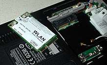
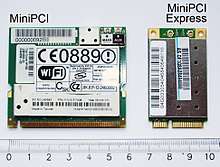
PCI Express Mini Card (also known as Mini PCI Express, Mini PCIe, Mini PCI-E, mPCIe, and PEM), based on PCI Express, is a replacement for the Mini PCI form factor. It is developed by the PCI-SIG. The host device supports both PCI Express and USB 2.0 connectivity, and each card may use either standard. Most laptop computers built after 2005 use PCI Express for expansion cards; however, as of 2015, many vendors are moving toward using the newer M.2 form factor for this purpose.
Due to different dimensions, PCI Express Mini Cards are not physically compatible with standard full-size PCI Express slots; however, passive adapters exist that let them be used in full-size slots.[27]
Physical dimensions
Dimensions of PCI Express Mini Cards are 30 mm x 50.95 mm (width x length) for a Full Mini Card. There is a 52-pin edge connector, consisting of two staggered rows on a 0.8 mm pitch. Each row has eight contacts, a gap equivalent to four contacts, then a further 18 contacts. Boards have a thickness of 1.0 mm, excluding the components. A "Half Mini Card" (sometimes abbreviated as HMC) is also specified, having approximately half the physical length of 26.8 mm.
Electrical interface
PCI Express Mini Card edge connectors provide multiple connections and buses:
Mini-SATA (mSATA) variant
Despite sharing the Mini PCI Express form factor, an mSATA slot is not necessarily electrically compatible with Mini PCI Express. For this reason, only certain notebooks are compatible with mSATA drives. Most compatible systems are based on Intel's Sandy Bridge processor architecture, using the Huron River platform. Notebooks such as Lenovo's ThinkPad T, W and X series, released in March–April 2011, have support for an mSATA SSD card in their WWAN card slot. The ThinkPad Edge E220s/E420s, and the Lenovo IdeaPad Y460/Y560/Y570/Y580 also support mSATA.[28]
Some notebooks (notably the Asus Eee PC, the Apple MacBook Air, and the Dell mini9 and mini10) use a variant of the PCI Express Mini Card as an SSD. This variant uses the reserved and several non-reserved pins to implement SATA and IDE interface passthrough, keeping only USB, ground lines, and sometimes the core PCIe x1 bus intact.[29] This makes the "miniPCIe" flash and solid-state drives sold for netbooks largely incompatible with true PCI Express Mini implementations.
Also, the typical Asus miniPCIe SSD is 71 mm long, causing the Dell 51 mm model to often be (incorrectly) referred to as half length. A true 51 mm Mini PCIe SSD was announced in 2009, with two stacked PCB layers that allow for higher storage capacity. The announced design preserves the PCIe interface, making it compatible with the standard mini PCIe slot. No working product has yet been developed.
Intel has numerous desktop boards with the PCIe x1 Mini-Card slot that typically do not support mSATA SSD. A list of desktop boards that natively support mSATA in the PCIe x1 Mini-Card slot (typically multiplexed with a SATA port) is provided on the Intel Support site.[30]
PCI Express M.2
M.2 replaces the mSATA standard and Mini PCIe[31]. Computer bus interfaces provided through the M.2 connector are PCI Express 3.0 (up to four lanes), Serial ATA 3.0, and USB 3.0 (a single logical port for each of the latter two). It is up to the manufacturer of the M.2 host or device to select which interfaces to support, depending on the desired level of host support and device type.
PCI Express External Cabling
PCI Express External Cabling (also known as External PCI Express, Cabled PCI Express, or ePCIe) specifications were released by the PCI-SIG in February 2007.[32][33]
Standard cables and connectors have been defined for x1, x4, x8, and x16 link widths, with a transfer rate of 250 MB/s per lane. The PCI-SIG also expects the norm will evolve to reach 500 MB/s, as in PCI Express 2.0. An example of the uses of Cabled PCI Express is a metal enclosure, containing a number of PCIe slots and PCIe-to-ePCIe adapter circuitry. This device would not be possible had it not been for the ePCIe spec.
PCI Express OCuLink
OCuLink (standing for "optical-copper link", since Cu is the chemical symbol for Copper) is an extension for the "cable version of PCI Express", acting as a competitor to version 3 of the Thunderbolt interface. Version 1.0 of OCuLink, released in Oct 2015, supports up to PCIe 3.0 x4 lanes (8 GT/s, 3.9 GB/s) over copper cabling; a fiber optic version may appear in the future.[34][35]
OCuLink, in the lastest version, has up to 16 GT/s (8 GB/s total for x4 lanes),[36] while the maximum bandwidth of a Thunderbolt 3 connector is 5 GB/s.
Derivative forms
Several other types of expansion card are derived from PCIe; these include:
- Low-height card
- ExpressCard: Successor to the PC Card form factor (with x1 PCIe and USB 2.0; hot-pluggable)
- PCI Express ExpressModule: A hot-pluggable modular form factor defined for servers and workstations
- XQD card: A PCI Express-based flash card standard by the CompactFlash Association with x2 PCIe
- CFexpress card: A PCI Express-based flash card by the CompactFlash Association in three form factors supporting 1 to 4 PCIe lanes
- SD card: The SD Express bus, introduced in version 7.0 of the SD specification uses an x1 PCIe link
- XMC: Similar to the CMC/PMC form factor (VITA 42.3)
- AdvancedTCA: A complement to CompactPCI for larger applications; supports serial based backplane topologies
- AMC: A complement to the AdvancedTCA specification; supports processor and I/O modules on ATCA boards (x1, x2, x4 or x8 PCIe).
- FeaturePak: A tiny expansion card format (43 x 65 mm) for embedded and small-form-factor applications, which implements two x1 PCIe links on a high-density connector along with USB, I2C, and up to 100 points of I/O
- Universal IO: A variant from Super Micro Computer Inc designed for use in low-profile rack-mounted chassis.[37] It has the connector bracket reversed so it cannot fit in a normal PCI Express socket, but it is pin-compatible and may be inserted if the bracket is removed.
- Thunderbolt: A variant from Intel that combines DisplayPort and PCIe protocols in a form factor compatible with Mini DisplayPort. Thunderbolt 3.0 also combines USB 3.1 and uses the USB-C form factor as opposed to Mini DisplayPort.
- Serial Digital Video Out: Some 9xx series Intel chipsets allow for adding another output for the integrated video into a PCIe slot (mostly dedicated and 16 lanes).
- M.2 (formerly known as NGFF)
- M-PCIe brings PCIe 3.0 to mobile devices (such as tablets and smartphones), over the M-PHY physical layer.[38][34]
- U.2 (formerly known as SFF-8639)
History and revisions
While in early development, PCIe was initially referred to as HSI (for High Speed Interconnect), and underwent a name change to 3GIO (for 3rd Generation I/O) before finally settling on its PCI-SIG name PCI Express. A technical working group named the Arapaho Work Group (AWG) drew up the standard. For initial drafts, the AWG consisted only of Intel engineers; subsequently, the AWG expanded to include industry partners.
Since, PCIe has undergone several large and smaller revisions, improving on performance and other features.
| PCI Express version |
Introduced | Line code |
Transfer rate[lower-roman 1][lower-roman 2] |
Throughput[lower-roman 1][lower-roman 3] | ||||
|---|---|---|---|---|---|---|---|---|
| x1 | x2 | x4 | x8 | x16 | ||||
| 1.0 | 2003 | 8b/10b | 2.5 GT/s | 250 MB/s | 0.500 GB/s | 1.00 GB/s | 2.0 GB/s | 4.0 GB/s |
| 2.0 | 2007 | 8b/10b | 5.0 GT/s | 500 MB/s | 1.000 GB/s | 2.00 GB/s | 4.0 GB/s | 8.0 GB/s |
| 3.0 | 2010 | 128b/130b | 8.0 GT/s | 984.6 MB/s | 1.969 GB/s | 3.94 GB/s | 7.88 GB/s | 15.75 GB/s |
| 4.0 | 2017 | 128b/130b | 16.0 GT/s | 1969 MB/s | 3.938 GB/s | 7.88 GB/s | 15.75 GB/s | 31.51 GB/s |
| 5.0 | 2019 | 128b/130b | 32.0 GT/s[lower-roman 4] | 3938 MB/s | 7.877 GB/s | 15.75 GB/s | 31.51 GB/s | 63.02 GB/s |
| 6.0 (planned) | 2021 | 128b/130b | 64.0 GT/s | 7877 MB/s | 15.754 GB/s | 31.51 GB/s | 63.02 GB/s | 126.03 GB/s |
- In each direction (each lane is a dual simplex channel).
- Transfer rate refers to the encoded serial bit rate; 2.5 GT/s means 2.5 Gbps serial data rate.
- Throughput refers to the pre-coded data rate prior to 8b/10b or 128b/130b coding. So transfer rate of 2.5 GT/s means 2.5 Gbit/s serial bit rate corresponding to a throughput of 2.0 Gbit/s or 250 MByte/s.
- Initially, 25.0 GT/s was also considered for technical feasibility.
PCI Express 1.0a
In 2003, PCI-SIG introduced PCIe 1.0a, with a per-lane data rate of 250 MB/s and a transfer rate of 2.5 gigatransfers per second (GT/s).
Transfer rate is expressed in transfers per second instead of bits per second because the number of transfers includes the overhead bits, which do not provide additional throughput;[41] PCIe 1.x uses an 8b/10b encoding scheme, resulting in a 20% (= 2/10) overhead on the raw channel bandwidth.[42] So in the PCIe terminology, transfer rate refers to the encoded bit rate: 2.5 GT/s is 2.5 Gbps on the encoded serial link. This corresponds to 2.0 Gbps of pre-coded data or 250 MB/s, which is referred to as throughput in PCIe.
PCI Express 1.1
In 2005, PCI-SIG[43] introduced PCIe 1.1. This updated specification includes clarifications and several improvements, but is fully compatible with PCI Express 1.0a. No changes were made to the data rate.
PCI Express 2.0
PCI-SIG announced the availability of the PCI Express Base 2.0 specification on 15 January 2007.[44] The PCIe 2.0 standard doubles the transfer rate compared with PCIe 1.0 to 5 GT/s and the per-lane throughput rises from 250 MB/s to 500 MB/s. Consequently, a 32-lane PCIe connector (x32) can support an aggregate throughput of up to 16 GB/s.
PCIe 2.0 motherboard slots are fully backward compatible with PCIe v1.x cards. PCIe 2.0 cards are also generally backward compatible with PCIe 1.x motherboards, using the available bandwidth of PCI Express 1.1. Overall, graphic cards or motherboards designed for v2.0 work, with the other being v1.1 or v1.0a.
The PCI-SIG also said that PCIe 2.0 features improvements to the point-to-point data transfer protocol and its software architecture.[45]
Intel's first PCIe 2.0 capable chipset was the X38 and boards began to ship from various vendors (Abit, Asus, Gigabyte) as of October 21, 2007.[46] AMD started supporting PCIe 2.0 with its AMD 700 chipset series and nVidia started with the MCP72.[47] All of Intel's prior chipsets, including the Intel P35 chipset, supported PCIe 1.1 or 1.0a.[48]
Like 1.x, PCIe 2.0 uses an 8b/10b encoding scheme, therefore delivering, per-lane, an effective 4 Gbit/s max transfer rate from its 5 GT/s raw data rate.
PCI Express 2.1
PCI Express 2.1 (with its specification dated March 4, 2009) supports a large proportion of the management, support, and troubleshooting systems planned for full implementation in PCI Express 3.0. However, the speed is the same as PCI Express 2.0. The increase in power from the slot breaks backward compatibility between PCI Express 2.1 cards and some older motherboards with 1.0/1.0a, but most motherboards with PCI Express 1.1 connectors are provided with a BIOS update by their manufacturers through utilities to support backward compatibility of cards with PCIe 2.1.
PCI Express 3.0
PCI Express 3.0 Base specification revision 3.0 was made available in November 2010, after multiple delays. In August 2007, PCI-SIG announced that PCI Express 3.0 would carry a bit rate of 8 gigatransfers per second (GT/s), and that it would be backward compatible with existing PCI Express implementations. At that time, it was also announced that the final specification for PCI Express 3.0 would be delayed until Q2 2010.[49] New features for the PCI Express 3.0 specification include a number of optimizations for enhanced signaling and data integrity, including transmitter and receiver equalization, PLL improvements, clock data recovery, and channel enhancements for currently supported topologies.[50]
Following a six-month technical analysis of the feasibility of scaling the PCI Express interconnect bandwidth, PCI-SIG's analysis found that 8 gigatransfers per second can be manufactured in mainstream silicon process technology, and can be deployed with existing low-cost materials and infrastructure, while maintaining full compatibility (with negligible impact) to the PCI Express protocol stack.
PCI Express 3.0 upgrades the encoding scheme to 128b/130b from the previous 8b/10b encoding, reducing the bandwidth overhead from 20% of PCI Express 2.0 to approximately 1.54% (= 2/130). A desirable balance of 0 and 1 bits in the data stream is achieved by XORing a known binary polynomial as a "scrambler" to the data stream in a feedback topology. Because the scrambling polynomial is known, the data can be recovered by applying the XOR a second time. Both the scrambling and descrambling steps are carried out in hardware. PCI Express 3.0's 8 GT/s bit rate effectively delivers 985 MB/s per lane, nearly doubling the lane bandwidth relative to PCI Express 2.0.[40]
On November 18, 2010, the PCI Special Interest Group officially published the finalized PCI Express 3.0 specification to its members to build devices based on this new version of PCI Express.[51]
PCI Express 3.1
In September 2013, PCI Express 3.1 specification was announced for release in late 2013 or early 2014, consolidating various improvements to the published PCI Express 3.0 specification in three areas: power management, performance and functionality.[34][52] It was released in November 2014.[53]
PCI Express 4.0
On November 29, 2011, PCI-SIG preliminarily announced PCI Express 4.0,[54] providing a 16 GT/s bit rate that doubles the bandwidth provided by PCI Express 3.0, while maintaining backward and forward compatibility in both software support and used mechanical interface.[55] PCI Express 4.0 specs also bring OCuLink-2, an alternative to Thunderbolt connector. OCuLink version 2 has up to 16 GT/s (8 GB/s total for x4 lanes),[36] while the maximum bandwidth of a Thunderbolt 3 connector is 5 GB/s.
In August 2016, Synopsys presented a test machine running PCIe 4.0 at the Intel Developer Forum. Their IP has been licensed to several firms planning to present their chips and products at the end of 2016.[56][57]
PCI-SIG officially announced the release of the final PCI Express 4.0 specification on June 8, 2017.[58] The spec includes improvements in flexibility, scalability, and lower-power.
NETINT Technologies introduced the first NVMe SSD based on PCIe 4.0 on July 17, 2018, ahead of Flash Memory Summit 2018[59]
Mellanox Technologies announced the first 100 Gbit network adapter with PCIe 4.0 on 15 June 2016,[60] and the first 200 Gbit network adapter with PCIe 4.0 on 10 November 2016.[61]
AMD announced on 9 January 2019 its upcoming Zen 2-based processors and X570 chipset would support PCIe 4.0.[62] AMD had hoped to enable partial support for older chipsets, but instability caused by motherboard traces not conforming to PCIe 4.0 specifications made that impossible.[63][64]
PCI Express 5.0
In June 2017, PCI-SIG announced the PCI Express 5.0 preliminary specification.[58] Bandwidth was expected to increase to 32 GT/s, yielding 63 GB/s in each direction in a 16-lane configuration. The draft spec was expected to be standardized in 2019. PLDA announced the availability of their XpressRICH5 PCIe 5.0 Controller IP based on draft 0.7 of the PCIe 5.0 specification on the same day.[65][66]
On 10 December 2018, the PCI SIG released version 0.9 of the PCIe 5.0 specification to its members,[67] and on 17 January 2019, PCI SIG announced the version 0.9 had been ratified, with version 1.0 targeted for release in the first quarter of 2019.[68]
On 29 May 2019, PCI-SIG officially announced the release of the final PCI-Express 5.0 specification.[69]
On 20 November 2019, Jiangsu Huacun presented the first PCIe 5.0 Controller HC9001 in a 12 nm manufacturing process.[70] The mass production is planned to start in 2020.
PCI Express 6.0
On June 18, 2019, PCI-SIG announced the development of PCI Express 6.0 specification. Bandwidth is expected to increase to 64 GT/s, yielding 128 GB/s in each direction in a 16-lane configuration, with a target release date of 2021.[71] The new standard uses 4-level pulse-amplitude modulation (PAM-4) with a low-latency forward error correction (FEC) in place of non-return-to-zero (NRZ) modulation.[72] Unlike previous PCI Express versions, forward error correction is used to increase data integrity and PAM-4 is used as line code so that two bits are transferred per transfer. With 64 GT/s data transfer rate (raw bit rate) and up to 256 GB/s via x16 configuration.[71]
Revision 0.5 as a "firstdraft" specification was released on 24 February 2020.[73]
Extensions and future directions
Some vendors offer PCIe over fiber products,[74][75][76] but these generally find use only in specific cases where transparent PCIe bridging is preferable to using a more mainstream standard (such as InfiniBand or Ethernet) that may require additional software to support it; current implementations focus on distance rather than raw bandwidth and typically do not implement a full x16 link.
Thunderbolt was co-developed by Intel and Apple as a general-purpose high speed interface combining a x4 PCIe link with DisplayPort and was originally intended as an all-fiber interface, but due to early difficulties in creating a consumer-friendly fiber interconnect, nearly all implementations are copper systems. A notable exception, the Sony VAIO Z VPC-Z2, uses a nonstandard USB port with an optical component to connect to an outboard PCIe display adapter. Apple has been the primary driver of Thunderbolt adoption through 2011, though several other vendors[77] have announced new products and systems featuring Thunderbolt. Thunderbolt 3 is part of the USB4 standard.
Mobile PCIe specification (abbreviated to M-PCIe) allows PCI Express architecture to operate over the MIPI Alliance's M-PHY physical layer technology. Building on top of already existing widespread adoption of M-PHY and its low-power design, Mobile PCIe lets mobile devices use PCI Express.[78]
Draft process
There are 5 primary releases/checkpoints in a PCI-SIG specification:[79]
- Draft 0.3 (Concept): this release may have few details, but outlines the general approach and goals.
- Draft 0.5 (First draft): this release has a complete set of architectural requirements and must fully address the goals set out in the 0.3 draft.
- Draft 0.7 (Complete draft): this release must have a complete set of functional requirements and methods defined, and no new functionality may be added to the specification after this release. Before the release of this draft, electrical specifications must have been validated via test silicon.
- Draft 0.9 (Final draft): this release allows PCI-SIG member companies to perform an internal review for intellectual property, and no functional changes are permitted after this draft.
- 1.0 (Final release): this is the final and definitive specification, and any changes or enhancements are through Errata documentation and Engineering Change Notices (ECNs) respectively.
Historically, the earliest adopters of a new PCIe specification generally begin designing with the Draft 0.5 as they can confidently build up their application logic around the new bandwidth definition and often even start developing for any new protocol features. At the Draft 0.5 stage, however, there is still a strong likelihood of changes in the actual PCIe protocol layer implementation, so designers responsible for developing these blocks internally may be more hesitant to begin work than those using interface IP from external sources.
Hardware protocol summary
The PCIe link is built around dedicated unidirectional couples of serial (1-bit), point-to-point connections known as lanes. This is in sharp contrast to the earlier PCI connection, which is a bus-based system where all the devices share the same bidirectional, 32-bit or 64-bit parallel bus.
PCI Express is a layered protocol, consisting of a transaction layer, a data link layer, and a physical layer. The Data Link Layer is subdivided to include a media access control (MAC) sublayer. The Physical Layer is subdivided into logical and electrical sublayers. The Physical logical-sublayer contains a physical coding sublayer (PCS). The terms are borrowed from the IEEE 802 networking protocol model.
Physical layer
| Lanes | Pins | Length | ||
|---|---|---|---|---|
| Total | Variable | Total | Variable | |
| x1 | 2x18 = 36[80] | 2x7 = 14 | 25 mm | 7.65 mm |
| x4 | 2x32 = 64 | 2x21 = 42 | 39 mm | 21.65 mm |
| x8 | 2x49 = 98 | 2x38 = 76 | 56 mm | 38.65 mm |
| x16 | 2x82 = 164 | 2x71 = 142 | 89 mm | 71.65 mm |

The PCIe Physical Layer (PHY, PCIEPHY, PCI Express PHY, or PCIe PHY) specification is divided into two sub-layers, corresponding to electrical and logical specifications. The logical sublayer is sometimes further divided into a MAC sublayer and a PCS, although this division is not formally part of the PCIe specification. A specification published by Intel, the PHY Interface for PCI Express (PIPE),[81] defines the MAC/PCS functional partitioning and the interface between these two sub-layers. The PIPE specification also identifies the physical media attachment (PMA) layer, which includes the serializer/deserializer (SerDes) and other analog circuitry; however, since SerDes implementations vary greatly among ASIC vendors, PIPE does not specify an interface between the PCS and PMA.
At the electrical level, each lane consists of two unidirectional differential pairs operating at 2.5, 5, 8 or 16 Gbit/s, depending on the negotiated capabilities. Transmit and receive are separate differential pairs, for a total of four data wires per lane.
A connection between any two PCIe devices is known as a link, and is built up from a collection of one or more lanes. All devices must minimally support single-lane (x1) link. Devices may optionally support wider links composed of 2, 4, 8, 12, 16, or 32 lanes. This allows for very good compatibility in two ways:
- A PCIe card physically fits (and works correctly) in any slot that is at least as large as it is (e.g., an x1 sized card works in any sized slot);
- A slot of a large physical size (e.g., x16) can be wired electrically with fewer lanes (e.g., x1, x4, x8, or x12) as long as it provides the ground connections required by the larger physical slot size.
In both cases, PCIe negotiates the highest mutually supported number of lanes. Many graphics cards, motherboards and BIOS versions are verified to support x1, x4, x8 and x16 connectivity on the same connection.
The width of a PCIe connector is 8.8 mm, while the height is 11.25 mm, and the length is variable. The fixed section of the connector is 11.65 mm in length and contains two rows of 11 (22 pins total), while the length of the other section is variable depending on the number of lanes. The pins are spaced at 1 mm intervals, and the thickness of the card going into the connector is 1.6 mm.[82][83]
Data transmission
PCIe sends all control messages, including interrupts, over the same links used for data. The serial protocol can never be blocked, so latency is still comparable to conventional PCI, which has dedicated interrupt lines. When the problem of IRQ sharing of pin based interrupts is taken into account and the fact that message signaled interrupts can bypass an I/O APIC and be delivered to the CPU directly, MSI performance ends up being substantially better. [84]
Data transmitted on multiple-lane links is interleaved, meaning that each successive byte is sent down successive lanes. The PCIe specification refers to this interleaving as data striping. While requiring significant hardware complexity to synchronize (or deskew) the incoming striped data, striping can significantly reduce the latency of the nth byte on a link. While the lanes are not tightly synchronized, there is a limit to the lane to lane skew of 20/8/6 ns for 2.5/5/8 GT/s so the hardware buffers can re-align the striped data.[85] Due to padding requirements, striping may not necessarily reduce the latency of small data packets on a link.
As with other high data rate serial transmission protocols, the clock is embedded in the signal. At the physical level, PCI Express 2.0 utilizes the 8b/10b encoding scheme[40] (line code) to ensure that strings of consecutive identical digits (zeros or ones) are limited in length. This coding was used to prevent the receiver from losing track of where the bit edges are. In this coding scheme every eight (uncoded) payload bits of data are replaced with 10 (encoded) bits of transmit data, causing a 20% overhead in the electrical bandwidth. To improve the available bandwidth, PCI Express version 3.0 instead uses 128b/130b encoding with scrambling. 128b/130b encoding relies on the scrambling to limit the run length of identical-digit strings in data streams and ensure the receiver stays synchronised to the transmitter. It also reduces electromagnetic interference (EMI) by preventing repeating data patterns in the transmitted data stream.
Data link layer
The data link layer performs three vital services for the PCIe express link:
- sequence the transaction layer packets (TLPs) that are generated by the transaction layer,
- ensure reliable delivery of TLPs between two endpoints via an acknowledgement protocol (ACK and NAK signaling) that explicitly requires replay of unacknowledged/bad TLPs,
- initialize and manage flow control credits
On the transmit side, the data link layer generates an incrementing sequence number for each outgoing TLP. It serves as a unique identification tag for each transmitted TLP, and is inserted into the header of the outgoing TLP. A 32-bit cyclic redundancy check code (known in this context as Link CRC or LCRC) is also appended to the end of each outgoing TLP.
On the receive side, the received TLP's LCRC and sequence number are both validated in the link layer. If either the LCRC check fails (indicating a data error), or the sequence-number is out of range (non-consecutive from the last valid received TLP), then the bad TLP, as well as any TLPs received after the bad TLP, are considered invalid and discarded. The receiver sends a negative acknowledgement message (NAK) with the sequence-number of the invalid TLP, requesting re-transmission of all TLPs forward of that sequence-number. If the received TLP passes the LCRC check and has the correct sequence number, it is treated as valid. The link receiver increments the sequence-number (which tracks the last received good TLP), and forwards the valid TLP to the receiver's transaction layer. An ACK message is sent to remote transmitter, indicating the TLP was successfully received (and by extension, all TLPs with past sequence-numbers.)
If the transmitter receives a NAK message, or no acknowledgement (NAK or ACK) is received until a timeout period expires, the transmitter must retransmit all TLPs that lack a positive acknowledgement (ACK). Barring a persistent malfunction of the device or transmission medium, the link-layer presents a reliable connection to the transaction layer, since the transmission protocol ensures delivery of TLPs over an unreliable medium.
In addition to sending and receiving TLPs generated by the transaction layer, the data-link layer also generates and consumes DLLPs, data link layer packets. ACK and NAK signals are communicated via DLLPs, as are some power management messages and flow control credit information (on behalf of the transaction layer).
In practice, the number of in-flight, unacknowledged TLPs on the link is limited by two factors: the size of the transmitter's replay buffer (which must store a copy of all transmitted TLPs until the remote receiver ACKs them), and the flow control credits issued by the receiver to a transmitter. PCI Express requires all receivers to issue a minimum number of credits, to guarantee a link allows sending PCIConfig TLPs and message TLPs.
Transaction layer
PCI Express implements split transactions (transactions with request and response separated by time), allowing the link to carry other traffic while the target device gathers data for the response.
PCI Express uses credit-based flow control. In this scheme, a device advertises an initial amount of credit for each received buffer in its transaction layer. The device at the opposite end of the link, when sending transactions to this device, counts the number of credits each TLP consumes from its account. The sending device may only transmit a TLP when doing so does not make its consumed credit count exceed its credit limit. When the receiving device finishes processing the TLP from its buffer, it signals a return of credits to the sending device, which increases the credit limit by the restored amount. The credit counters are modular counters, and the comparison of consumed credits to credit limit requires modular arithmetic. The advantage of this scheme (compared to other methods such as wait states or handshake-based transfer protocols) is that the latency of credit return does not affect performance, provided that the credit limit is not encountered. This assumption is generally met if each device is designed with adequate buffer sizes.
PCIe 1.x is often quoted to support a data rate of 250 MB/s in each direction, per lane. This figure is a calculation from the physical signaling rate (2.5 gigabaud) divided by the encoding overhead (10 bits per byte). This means a sixteen lane (x16) PCIe card would then be theoretically capable of 16x250 MB/s = 4 GB/s in each direction. While this is correct in terms of data bytes, more meaningful calculations are based on the usable data payload rate, which depends on the profile of the traffic, which is a function of the high-level (software) application and intermediate protocol levels.
Like other high data rate serial interconnect systems, PCIe has a protocol and processing overhead due to the additional transfer robustness (CRC and acknowledgements). Long continuous unidirectional transfers (such as those typical in high-performance storage controllers) can approach >95% of PCIe's raw (lane) data rate. These transfers also benefit the most from increased number of lanes (x2, x4, etc.) But in more typical applications (such as a USB or Ethernet controller), the traffic profile is characterized as short data packets with frequent enforced acknowledgements.[86] This type of traffic reduces the efficiency of the link, due to overhead from packet parsing and forced interrupts (either in the device's host interface or the PC's CPU). Being a protocol for devices connected to the same printed circuit board, it does not require the same tolerance for transmission errors as a protocol for communication over longer distances, and thus, this loss of efficiency is not particular to PCIe.
Applications

PCI Express operates in consumer, server, and industrial applications, as a motherboard-level interconnect (to link motherboard-mounted peripherals), a passive backplane interconnect and as an expansion card interface for add-in boards.
In virtually all modern (as of 2012) PCs, from consumer laptops and desktops to enterprise data servers, the PCIe bus serves as the primary motherboard-level interconnect, connecting the host system-processor with both integrated-peripherals (surface-mounted ICs) and add-on peripherals (expansion cards). In most of these systems, the PCIe bus co-exists with one or more legacy PCI buses, for backward compatibility with the large body of legacy PCI peripherals.
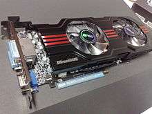
As of 2013 PCI Express has replaced AGP as the default interface for graphics cards on new systems. Almost all models of graphics cards released since 2010 by AMD (ATI) and Nvidia use PCI Express. Nvidia uses the high-bandwidth data transfer of PCIe for its Scalable Link Interface (SLI) technology, which allows multiple graphics cards of the same chipset and model number to run in tandem, allowing increased performance. AMD has also developed a multi-GPU system based on PCIe called CrossFire. AMD, Nvidia, and Intel have released motherboard chipsets that support as many as four PCIe x16 slots, allowing tri-GPU and quad-GPU card configurations.
Note that special power cables called PCI-e power cables are required for high-end graphics cards.[87]
External GPUs
Theoretically, external PCIe could give a notebook the graphics power of a desktop, by connecting a notebook with any PCIe desktop video card (enclosed in its own external housing, with a power supply and cooling); this is possible with an ExpressCard interface or a Thunderbolt interface. The ExpressCard interface provides bit rates of 5 Gbit/s (0.5 GB/s throughput), whereas the Thunderbolt interface provides bit rates of up to 40 Gbit/s (5 GB/s throughput).
In 2006, Nvidia developed the Quadro Plex external PCIe family of GPUs that can be used for advanced graphic applications for the professional market.[88] These video cards require a PCI Express x8 or x16 slot for the host-side card, which connects to the Plex via a VHDCI carrying eight PCIe lanes.[89]
In 2008, AMD announced the ATI XGP technology, based on a proprietary cabling system that is compatible with PCIe x8 signal transmissions.[90] This connector is available on the Fujitsu Amilo and the Acer Ferrari One notebooks. Fujitsu launched their AMILO GraphicBooster enclosure for XGP soon thereafter.[91] Around 2010 Acer launched the Dynavivid graphics dock for XGP.[92]
In 2010 external card hubs were introduced that can connect to a laptop or desktop through a PCI ExpressCard slot. These hubs can accept full-sized graphics cards. Examples include MSI GUS,[93] Village Instrument's ViDock,[94] the Asus XG Station, Bplus PE4H V3.2 adapter,[95] as well as more improvised DIY devices.[96] However such solutions are limited by the size (often only x1) and version of the available PCIe slot on a laptop.
Intel Thunderbolt interface has given opportunity to new and faster products to connect with a PCIe card externally. Magma has released the ExpressBox 3T, which can hold up to three PCIe cards (two at x8 and one at x4).[97] MSI also released the Thunderbolt GUS II, a PCIe chassis dedicated for video cards.[98] Other products such as the Sonnet's Echo Express[99] and mLogic's mLink are Thunderbolt PCIe chassis in a smaller form factor.[100] However, all these products require a computer with a Thunderbolt port (i.e., Thunderbolt devices), such as Apple's MacBook Pro models released in late 2013.
In 2017, more fully featured external card hubs were introduced, such as the Razer Core, which has a full-length PCIe x16 interface.[101]
Storage devices

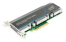
PCI Express protocol can be used as data interface to flash memory devices, such as memory cards and solid-state drives (SSDs).
XQD card is a memory card format utilizing PCI Express, developed by the CompactFlash Association, with transfer rates of up to 500 MB/s.[102]
Many high-performance, enterprise-class SSDs are designed as PCI Express RAID controller cards with flash memory chips placed directly on the circuit board, utilizing proprietary interfaces and custom drivers to communicate with the operating system; this allows much higher transfer rates (over 1 GB/s) and IOPS (over one million I/O operations per second) when compared to Serial ATA or SAS drives.[103][104] For example, in 2011 OCZ and Marvell co-developed a native PCI Express solid-state drive controller for a PCI Express 3.0 x16 slot with maximum capacity of 12 TB and a performance of to 7.2 GB/s sequential transfers and up to 2.52 million IOPS in random transfers.[105]
SATA Express is an interface for connecting SSDs, by providing multiple PCI Express lanes as a pure PCI Express connection to the attached storage device.[106] M.2 is a specification for internally mounted computer expansion cards and associated connectors, which also uses multiple PCI Express lanes.[107]
PCI Express storage devices can implement both AHCI logical interface for backward compatibility, and NVM Express logical interface for much faster I/O operations provided by utilizing internal parallelism offered by such devices. Enterprise-class SSDs can also implement SCSI over PCI Express.[108]
Cluster interconnect
Certain data-center applications (such as large computer clusters) require the use of fiber-optic interconnects due to the distance limitations inherent in copper cabling. Typically, a network-oriented standard such as Ethernet or Fibre Channel suffices for these applications, but in some cases the overhead introduced by routable protocols is undesirable and a lower-level interconnect, such as InfiniBand, RapidIO, or NUMAlink is needed. Local-bus standards such as PCIe and HyperTransport can in principle be used for this purpose,[109] but as of 2015 solutions are only available from niche vendors such as Dolphin ICS.
Competing protocols
Other communications standards based on high bandwidth serial architectures include InfiniBand, RapidIO, HyperTransport, Intel QuickPath Interconnect, and the Mobile Industry Processor Interface (MIPI). The differences are based on the trade-offs between flexibility and extensibility vs latency and overhead. For example, making the system hot-pluggable, as with Infiniband but not PCI Express, requires that software track network topology changes.
Another example is making the packets shorter to decrease latency (as is required if a bus must operate as a memory interface). Smaller packets mean packet headers consume a higher percentage of the packet, thus decreasing the effective bandwidth. Examples of bus protocols designed for this purpose are RapidIO and HyperTransport.
PCI Express falls somewhere in the middle, targeted by design as a system interconnect (local bus) rather than a device interconnect or routed network protocol. Additionally, its design goal of software transparency constrains the protocol and raises its latency somewhat.
Delays in PCIe 4.0 implementations led to the Gen-Z consortium, the CCIX effort and an open Coherent Accelerator Processor Interface (CAPI) all being announced by the end of 2016.[110]
On March 11, 2019, Intel presented Compute Express Link (CXL), a new interconnect bus, based on the PCI Express 5.0 physical layer infrastructure. The initial promoters of the CXL specification included: Alibaba, Cisco, Dell EMC, Facebook, Google, HPE, Huawei, Intel and Microsoft.[111]
Integrators List
Integrators List is the Compliance Program power by PCI-SIG, This list includes all products that have successfully completed the rigorous testing procedures of the Compliance Workshop. Inclusion on the list is only available to PCI-SIG member companies and cannot be used for individual marketing programs. The list include Switches/Bridges, NIC, SSD etc. However, many companies do refer to the list when making company-to-company purchases.[112]
See also
- Active State Power Management (ASPM)
- Conventional PCI
- PCI configuration space
- PCI-X
- PCI/104-Express
- PCIe/104
- Root complex
- Serial Digital Video Out (SDVO)
- List of device bit rates § Main buses
Notes
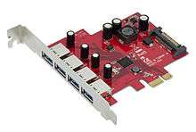
- The card's Serial ATA power connector is present because the USB 3.0 ports require more power than the PCI Express bus can supply. More often, a 4-pin Molex power connector is used.
References
- "PCI express and advanced switching: Evolutionary path to building next generation interconnects". August 2003: 21–29. doi:10.1109/CONECT.2003.1231473. Cite journal requires
|journal=(help) - "Definition of PCI Express".
- Zhang, Yanmin; Nguyen, T Long (June 2007). "Enable PCI Express Advanced Error Reporting in the Kernel" (PDF). Proceedings of the Linux Symposium. Fedora project. Archived (PDF) from the original on 2016-03-10.
- https://www.hyperstone.com Flash Memory Form Factors - The Fundamentals of Reliable Flash Storage, Retrieved 19 April 2018
- Ravi Budruk (2007-08-21). "PCI Express Basics". PCI-SIG. Archived from the original (PDF) on 2014-07-15. Retrieved 2014-07-15.
- "How PCI Express Works". How Stuff Works. 2005-08-17. Archived from the original on 2009-12-03. Retrieved 2009-12-07.
- These bus widths are only mentioned in this white paper (and in numerous copies of this document). The standard itself defines only 1, 4, 8 and 16 lanes and their mechanical properties. There are two tracks in the M.2/NGFF standard with A, B or E encoded devices.
- "PCI Express Architecture Frequently Asked Questions". PCI-SIG. Archived from the original on 13 November 2008. Retrieved 23 November 2008.
- "PCI Express Bus". Interface bus. Archived from the original on 2007-12-08. Retrieved 2010-06-12.
- 32 lanes are defined by the PCIe Base Specification but there's no card standard in the PCIe Card Electromechanical Specification.
- "PCI Express – An Overview of the PCI Express Standard". Developer Zone. National Instruments. 2009-08-13. Archived from the original on 2010-01-05. Retrieved 2009-12-07.
- Qazi, Atif. "What are PCIe Slots?". PC Gear Lab. Retrieved 8 April 2020.
- "New PCIe Form Factor Enables Greater PCIe SSD Adoption". NVM Express. 12 June 2012. Archived from the original on 6 September 2015.
- "Memblaze PBlaze4 AIC NVMe SSD Review". StorageReview. 21 December 2015.
- "Sapphire Radeon RX 5700 XT Pulse Review | bit-tech.net". bit-tech.net. Retrieved 2019-08-26.
- "AMD Radeon™ RX 5700 XT 8GB GDDR6 THICC II - RX-57XT8DFD6". xfxforce.com. Retrieved 2019-08-25.
- "What is the A side, B side configuration of PCI cards". Frequently Asked Questions. Adex Electronics. 1998. Archived from the original on 2011-11-02. Retrieved Oct 24, 2011.
- PCI Express Card Electromechanical Specification Revision 2.0
- "L1 PM Substates with CLKREQ, Revision 1.0a" (PDF). PCI-SIG. Retrieved 2018-11-08.
- "Emergency Power Reduction Mechanism with PWRBRK Signal ECN" (PDF). PCI-SIG. Retrieved 2018-11-08.
- PCI Express Card Electromechanical Specification Revision 1.1
- Schoenborn, Zale (2004), Board Design Guidelines for PCI Express Architecture (PDF), PCI-SIG, pp. 19–21, archived (PDF) from the original on 2016-03-27
- PCI Express x16 Graphics 150W-ATX Specification Revision 1.0
- PCI Express 225 W/300 W High Power Card Electromechanical Specification Revision 1.0
- PCI Express Card Electromechanical Specification Revision 3.0
- Yun Ling (2008-05-16). "PCIe Electromechanical Updates". Archived from the original on 2015-11-05. Retrieved 2015-11-07.
- "MP1: Mini PCI Express / PCI Express Adapter". hwtools.net. 2014-07-18. Archived from the original on 2014-10-03. Retrieved 2014-09-28.
- "mSATA FAQ: A Basic Primer". Notebook review. Archived from the original on 2012-02-12.
- "Eee PC Research". ivc (wiki). Archived from the original on 30 March 2010. Retrieved 26 October 2009.
- "Desktop Board Solid-state drive (SSD) compatibility". Intel. Archived from the original on 2016-01-02.
- "How to distinguish the differences between M.2 cards | Dell US". www.dell.com. Retrieved 2020-03-24.
- "PCI Express External Cabling 1.0 Specification". Archived from the original on 10 February 2007. Retrieved 9 February 2007.
- "PCI Express External Cabling Specification Completed by PCI-SIG". PCI SIG. 2007-02-07. Archived from the original on 2013-11-26. Retrieved 2012-12-07.
- "PCI SIG discusses M‐PCIe oculink & 4th gen PCIe", The Register, UK, September 13, 2013, archived from the original on June 29, 2017
- Anton Shilov. PCI SIG to finalize OCuLink external PCI Express this fall Archived 2015-06-27 at the Wayback Machine. KitGuru. June 26th, 2015
- OCuLink 2nd gen Archived 2017-03-13 at the Wayback Machine
- "Supermicro Universal I/O (UIO) Solutions". Supermicro.com. Archived from the original on 2014-03-24. Retrieved 2014-03-24.
- "Get ready for M-PCIe testing", PC board design, EDN
- "PCI Express 4.0 Frequently Asked Questions". pcisig.com. PCI-SIG. Archived from the original on 2014-05-18. Retrieved 2014-05-18.
- "PCI Express 3.0 Frequently Asked Questions". pcisig.com. PCI-SIG. Archived from the original on 2014-02-01. Retrieved 2014-05-01.
- "What does GT/s mean, anyway?". TM World. Archived from the original on 2012-08-14. Retrieved 2012-12-07.
- "Deliverable 12.2". SE: Eiscat. Archived from the original on 2010-08-17. Retrieved 2012-12-07.
- PCI SIG, archived from the original on 2008-07-06
- "PCI Express Base 2.0 specification announced" (PDF) (Press release). PCI-SIG. 15 January 2007. Archived from the original (PDF) on 4 March 2007. Retrieved 9 February 2007. — note that in this press release the term aggregate bandwidth refers to the sum of incoming and outgoing bandwidth; using this terminology the aggregate bandwidth of full duplex 100BASE-TX is 200 Mbit/s.
- Smith, Tony (11 October 2006). "PCI Express 2.0 final draft spec published". The Register. Archived from the original on 29 January 2007. Retrieved 9 February 2007.
- Key, Gary; Fink, Wesley (21 May 2007). "Intel P35: Intel's Mainstream Chipset Grows Up". AnandTech. Archived from the original on 23 May 2007. Retrieved 21 May 2007.
- Huynh, Anh (8 February 2007). "NVIDIA "MCP72" Details Unveiled". AnandTech. Archived from the original on 10 February 2007. Retrieved 9 February 2007.
- "Intel P35 Express Chipset Product Brief" (PDF). Intel. Archived (PDF) from the original on 26 September 2007. Retrieved 5 September 2007.
- Hachman, Mark (2009-08-05). "PCI Express 3.0 Spec Pushed Out to 2010". PC Mag. Archived from the original on 2014-01-07. Retrieved 2012-12-07.
- "PCI Express 3.0 Bandwidth: 8.0 Gigatransfers/s". ExtremeTech. 9 August 2007. Archived from the original on 24 October 2007. Retrieved 5 September 2007.
- "PCI Special Interest Group Publishes PCI Express 3.0 Standard". X bit labs. 18 November 2010. Archived from the original on 21 November 2010. Retrieved 18 November 2010.
- "PCIe 3.1 and 4.0 Specifications Revealed". eteknix.com. Archived from the original on 2016-02-01.
- "Trick or Treat… PCI Express 3.1 Released!". synopsys.com. Archived from the original on 2015-03-23.
- "PCI Express 4.0 evolution to 16 GT/s, twice the throughput of PCI Express 3.0 technology" (press release). PCI-SIG. 2011-11-29. Archived from the original on 2012-12-23. Retrieved 2012-12-07.
- https://pcisig.com/faq?field_category_value%5B%5D=pci_express_4.0#4415 Archived 2016-10-20 at the Wayback Machine
- "PCIe 4.0 Heads to Fab, 5.0 to Lab". EE Times. 2016-06-26. Archived from the original on 2016-08-28. Retrieved 2016-08-27.
- "Archived copy". Archived from the original on 2016-08-19. Retrieved 2016-08-18.CS1 maint: archived copy as title (link)
- Born, Eric (8 June 2017). "PCIe 4.0 specification finally out with 16 GT/s on tap". Tech Report. Archived from the original on 8 June 2017. Retrieved 8 June 2017.
- "NETINT Introduces Codensity with Support for PCIe 4.0 - NETINT Technologies". NETINT Technologies. 2018-07-17. Retrieved 2018-09-28.
- https://www.mellanox.com/page/press_release_item?id=1737
- https://www.mellanox.com/page/press_release_item?id=1810
- https://wccftech.com/amd-ryzen-3000-zen-2-desktop-am4-processors-launching-mid-2019/
- Alcorn, Paul (3 June 2019). "AMD Nixes PCIe 4.0 Support on Older Socket AM4 Motherboards, Here's Why". Tom's Hardware. Archived from the original on 10 June 2019. Retrieved 10 June 2019.
- Alcorn, Paul (10 January 2019). "PCIe 4.0 May Come to all AMD Socket AM4 Motherboards (Updated)". Tom's Hardware. Archived from the original on 10 June 2019. Retrieved 10 June 2019.
- "PLDA Announces Availability of XpressRICH5™ PCIe 5.0 Controller IP | PLDA.com". www.plda.com. Retrieved 2018-06-28.
- "XpressRICH5 for ASIC | PLDA.com". www.plda.com. Retrieved 2018-06-28.
- "Doubling Bandwidth in Under Two Years: PCI Express® Base Specification Revision 5.0, Version 0.9 is Now Available to Members". pcisig.com. Retrieved 2018-12-12.
- "PCIe 5.0 Is Ready For Prime Time". tomshardware.com. Retrieved 18 January 2019.
- https://www.businesswire.com/news/home/20190529005766/en/PCI-SIG%C2%AE-Achieves-32GTs-New-PCI-Express%C2%AE-5.0
- https://www.pcgameshardware.de/Mainboard-Hardware-154107/News/PCI-Express50-China-stellt-ersten-Controller-vor-1337072/
- https://www.businesswire.com/news/home/20190618005945/en/PCI-SIG%C2%AE-Announces-Upcoming-PCI-Express%C2%AE-6.0-Specification
- https://www.anandtech.com/show/14559/pci-express-bandwidth-to-be-doubled-again-pcie-60-announced-spec-to-land-in-2021
- https://www.phoronix.com/scan.php?page=news_item&px=PCI-Express-6.0-v0.5
- "PLX demo shows PCIe over fiber as data center clustering interconnect". Cabling install. Penn Well. Retrieved 29 August 2012.
- "Introduced second generation PCI Express Gen 2 over fiber optic systems". Adnaco. 2011-04-22. Archived from the original on 4 October 2012. Retrieved 29 August 2012.
- "PCIe Active Optical Cable System". Archived from the original on 30 December 2014. Retrieved 23 October 2015.
- "Acer, Asus to Bring Intel's Thunderbolt Speed Technology to Windows PCs". PC World. 2011-09-14. Archived from the original on 2012-01-18. Retrieved 2012-12-07.
- Kevin Parrish (2013-06-28). "PCIe for Mobile Launched; PCIe 3.1, 4.0 Specs Revealed". Tom's Hardware. Retrieved 2014-07-10.
- "PCI Express 4.0 Draft 0.7 & PIPE 4.4 Specifications - What Do They Mean to Designers? — Synopsys Technical Article | ChipEstimate.com". www.chipestimate.com. Retrieved 2018-06-28.
- "PCI Express 1x, 4x, 8x, 16x bus pinout and wiring @". RU: Pinouts. Archived from the original on 2009-11-25. Retrieved 2009-12-07.
- "PHY Interface for the PCI Express Architecture" (PDF) (version 2.00 ed.). Intel. Archived from the original (PDF) on 17 March 2008. Retrieved 21 May 2008.
- "Mechanical Drawing for PCI Express Connector". Interface bus. Retrieved 7 December 2007.
- "FCi schematic for PCIe connectors" (PDF). FCI connect. Retrieved 7 December 2007.
- <
- PCI EXPRESS BASE SPECIFICATION, REV. 3.0 Table 4-24
- "Computer Peripherals And Interfaces". Technical Publications Pune. Archived from the original on 25 February 2014. Retrieved 23 July 2009.
- "All about the various PC power supply cables and connectors". www.playtool.com. Retrieved 2018-11-10.
- "NVIDIA Introduces NVIDIA Quadro® Plex – A Quantum Leap in Visual Computing". Nvidia. 2006-08-01. Archived from the original on 2006-08-24.
- "Quadro Plex VCS – Advanced visualization and remote graphics". nVidia. Archived from the original on 2011-04-28. Retrieved 2010-09-11.
- "XGP". ATI. AMD. Archived from the original on 2010-01-29. Retrieved 2010-09-11.
- Fujitsu-Siemens Amilo GraphicBooster External Laptop GPU Released, 2008-12-03, archived from the original on 2015-10-16, retrieved 2015-08-09
- DynaVivid Graphics Dock from Acer arrives in France, what about the US?, 2010-08-11, archived from the original on 2015-10-16, retrieved 2015-08-09
- Dougherty, Steve (May 22, 2010), "MSI to showcase 'GUS' external graphics solution for laptops at Computex", TweakTown
- Hellstrom, Jerry (August 9, 2011), "ExpressCard trying to pull a (not so) fast one?", PC Perspective (editorial), archived from the original on February 1, 2016
- "PE4H V3.2 (PCIe x16 Adapter)". Hwtools.net. Archived from the original on 2014-02-14. Retrieved 2014-02-05.
- O'Brien, Kevin (September 8, 2010), "How to Upgrade Your Notebook Graphics Card Using DIY ViDOCK", Notebook review, archived from the original on December 13, 2013
- Lal Shimpi, Anand (September 7, 2011), "The Thunderbolt Devices Trickle In: Magma's ExpressBox 3T", AnandTech, archived from the original on March 4, 2016
- "MSI GUS II external GPU enclosure with Thunderbolt". The Verge (hands-on). Archived from the original on 2012-02-13. Retrieved 2012-02-12.
- "PCI express graphics, Thunderbolt", Tom’s hardware
- "M logics M link Thunderbold chassis no shipping", Engadget, Dec 13, 2012, archived from the original on 2017-06-25
- Burns, Chris (October 17, 2017), "2017 Razer Blade Stealth and Core V2 detailed", SlashGear, archived from the original on October 17, 2017
- "CompactFlash Association readies next-gen XQD format, promises write speeds of 125 MB/s and up". Engadget. 2011-12-08. Archived from the original on 2014-05-19. Retrieved 2014-05-18.
- Zsolt Kerekes (December 2011). "What's so very different about the design of Fusion-io's ioDrives / PCIe SSDs?". storagesearch.com. Archived from the original on 2013-09-23. Retrieved 2013-10-02.
- "Fusion-io ioDrive Duo Enterprise PCIe Review". storagereview.com. 2012-07-16. Archived from the original on 2013-10-04. Retrieved 2013-10-02.
- "OCZ Demos 4 TiB, 16 TiB Solid-State Drives for Enterprise". X-bit labs. Archived from the original on 2013-03-25. Retrieved 2012-12-07.
- "Enabling Higher Speed Storage Applications with SATA Express". SATA-IO. Archived from the original on 2012-11-27. Retrieved 2012-12-07.
- "SATA M.2 Card". SATA-IO. Archived from the original on 2013-10-03. Retrieved 2013-09-14.
- "SCSI Express". SCSI Trade Association. Archived from the original on 2013-01-27. Retrieved 2012-12-27.
- Meduri, Vijay (2011-01-24). "A Case for PCI Express as a High-Performance Cluster Interconnect". HPCwire. Archived from the original on 2013-01-14. Retrieved 2012-12-07.
- Evan Koblentz (February 3, 2017). "New PCI Express 4.0 delay may empower next-gen alternatives". Tech Republic. Archived from the original on April 1, 2017. Retrieved March 31, 2017.
- Cutress, Ian. "CXL Specification 1.0 Released: New Industry High-Speed Interconnect From Intel". www.anandtech.com. Retrieved 2019-08-09.
- "Integrators List | PCI-SIG". pcisig.com. Retrieved 2019-03-27.
Further reading
- Budruk, Ravi; Anderson, Don; Shanley, Tom (2003), Winkles, Joseph ‘Joe’ (ed.), PCI Express System Architecture, Mind share PC system architecture, Addison-Wesley, ISBN 978-0-321-15630-3, 1120 pp.
- Solari, Edward; Congdon, Brad (2003), Complete PCI Express Reference: Design Implications for Hardware and Software Developers, Intel, ISBN 978-0-9717861-9-6, 1056 pp.
- Wilen, Adam; Schade, Justin P; Thornburg, Ron (Apr 2003), Introduction to PCI Express: A Hardware and Software Developer's Guide, Intel, ISBN 978-0-9702846-9-3, 325 pp.
Technical and de facto standards for wired computer buses | |
|---|---|
| General |
|
| Standards |
|
| Storage |
|
| Peripheral |
|
| Audio |
|
| Portable |
|
| Embedded |
|
Interfaces are listed by their speed in the (roughly) ascending order, so the interface at the end of each section should be the fastest. | |