Thermoelectric materials
Thermoelectric materials [1] show the thermoelectric effect in a strong or convenient form.
| Thermoelectric effect |
|---|
 |
|
Principles
|
The thermoelectric effect refers to phenomena by which either a temperature difference creates an electric potential or an electric potential creates a temperature difference. These phenomena are known more specifically as the Seebeck effect (creating a voltage from temperature difference), Peltier effect (driving heat flow with an electric current), and Thomson effect (reversible heating or cooling within a conductor when there is both an electric current and a temperature gradient). While all materials have a nonzero thermoelectric effect, in most materials it is too small to be useful. However, low-cost materials that have a sufficiently strong thermoelectric effect (and other required properties) are also considered for applications including power generation and refrigeration. The most commonly used thermoelectric material is based on bismuth telluride (Bi
2Te
3).
Thermoelectric materials are used in thermoelectric systems for cooling or heating in niche applications, and are being studied as a way to regenerate electricity from waste heat.[2]
Thermoelectric Figure of Merit
The usefulness of a material in thermoelectric systems is determined by the device efficiency. These are determined by the material's electrical conductivity, thermal conductivity, Seebeck coefficient which change with temperature. The maximum efficiency of a thermoelectric material is determined by its thermoelectric figure of merit. The maximum efficiency of the energy conversion process (for both power generation and cooling) at a given point in the material is determined by the thermoelectric materials figure of merit , given by [3]

- , which contains the Seebeck coefficient S, thermal conductivity κ, electrical conductivity σ, and temperature T.

Device efficiency
The efficiency of a thermoelectric device for electricity generation is given by , defined as


The maximum efficiency of a thermoelectric device is typically described in terms of its device figure of merit where the maximum device efficiency is given by


where is the temperature at the hot junction and is the temperature at the surface being cooled.


For a single thermoelectric leg the device efficiency can be calculated from the temperature dependent properties S, κ and σ and the heat and electrical current flow through the material.[4] In an actual thermoelectric device, two materials are used (typically one n-type and one p-type) with metal interconnects. The maximum efficiency is then calculated from the efficiency of both legs and the electrical and thermal losses from the interconnects and surroundings.

Ignoring these losses, an inexact estimate for is given by [5]

where is the electrical resistivity, and the properties are averaged over the temperature range; is the average temperature between the hot and cold surfaces and the subscripts n and p denote properties related to the n- and p-type semiconducting thermoelectric materials, respectively. Only when n and p elements have the same and temperature independent properties () does .


Since thermoelectric devices are heat engines, their efficiency is limited by the Carnot efficiency , the first factor in , while and determines the maximum reversibility of the thermodynamic process globally and locally, respectively. Regardless, the coefficient of performance of current commercial thermoelectric refrigerators ranges from 0.3 to 0.6, one-sixth the value of traditional vapor-compression refrigerators.[6]

Power factor
Often the thermoelectric power factor is reported for a thermoelectric material, given by:

where S is the Seebeck coefficient, and σ is the electrical conductivity.
Although it is often claimed that TE devices with materials with a higher power factor are able to 'generate' more energy (move more heat or extract more energy from that temperature difference) this is only true for a thermoelectric device with fixed geometry and unlimited heat source and cooling. If the geometry of the device is optimally designed for the specific application, the thermoelectric materials will operate at their peak efficiency which is determined by their not .[7]

Aspects of materials choice
For good efficiency, materials with high electrical conductivity, low thermal conductivity and high Seebeck coefficient are needed.
State density: metals vs semiconductors
The band structure of semiconductors offers better thermoelectric effects than the band structure of metals.
The Fermi energy is below the conduction band causing the state density to be asymmetric around the Fermi energy. Therefore, the average electron energy of the conduction band is higher than the Fermi energy, making the system conducive for charge motion into a lower energy state. By contrast, the Fermi energy lies in the conduction band in metals. This makes the state density symmetric about the Fermi energy so that the average conduction electron energy is close to the Fermi energy, reducing the forces pushing for charge transport. Therefore, semiconductors are ideal thermoelectric materials.[8]
Conductivity
In the efficiency equations above, thermal conductivity and electrical conductivity compete.
The thermal conductivity κ has mainly two components:
- κ = κ electron + κ phonon
According to the Wiedemann–Franz law, the higher the electrical conductivity, the higher κ electron becomes.[8] Thus in metals the ratio of thermal to electrical conductivity is about fixed, as the electron part dominates. In semiconductors, the phonon part is important and can not be neglected. It reduces the efficiency. For good efficiency a low ratio of κ phonon / κ electron is desired.
Therefore, it is necessary to minimize κ phonon and keep the electrical conductivity high. Thus semiconductors should be highly doped.
G. A. Slack[9] proposed that in order to optimize the figure of merit, phonons, which are responsible for thermal conductivity must experience the material as a glass (experiencing a high degree of phonon scattering—lowering thermal conductivity) while electrons must experience it as a crystal (experiencing very little scattering—maintaining electrical conductivity). The figure of merit can be improved through the independent adjustment of these properties.
Quality Factor (detailed theory on semiconductors)
The maximum of a material is given by the material's Quality Factor:


where is the Boltzmann constant, is the reduced Planck constant, is the number of degenerated valleys for the band, is the average longitudinal elastic moduli, is the inertial effective mass, is the deformation potential coefficient, is the lattice thermal conduction, and is temperature. The figure of merit, , depends on doping concentration and temperature of the material of interest.[10] The material Quality Factor: is useful because it allows for an intrinsic comparisons of possible efficiency between different materials.[11] This relation shows that improving the electronic component , which primarily affects the Seebeck coefficient, will increase the quality factor of a material. A large density of states can be created due to a large number of conducting bands () or by flat bands giving a high band effective mass (). For isotropic materials . Therefore, it is desirable for thermoelectric materials to have high valley degeneracy in a very sharp band structure.[12] Other complex features of the electronic structure are important. These can be partially quantified using an electronic fitness function.[13]


Materials of interest
Strategies to improve thermoelectrics include both advanced bulk materials and the use of low-dimensional systems. Such approaches to reduce lattice thermal conductivity fall under three general material types: (1) Alloys: create point defects, vacancies, or rattling structures (heavy-ion species with large vibrational amplitudes contained within partially filled structural sites) to scatter phonons within the unit cell crystal;[14] (2) Complex crystals: separate the phonon glass from the electron crystal using approaches similar to those for superconductors (the region responsible for electron transport should be an electron crystal of a high-mobility semiconductor, while the phonon glass should ideally house disordered structures and dopants without disrupting the electron crystal, analogous to the charge reservoir in high-Tc superconductors[15]); (3) Multiphase nanocomposites: scatter phonons at the interfaces of nanostructured materials,[16] be they mixed composites or thin film superlattices.
Materials under consideration for thermoelectric device applications include:
Bismuth chalcogenides and their nanostructures
Materials such as Bi
2Te
3 and Bi
2Se
3 comprise some of the best performing room temperature thermoelectrics with a temperature-independent figure-of-merit, ZT, between 0.8 and 1.0.[17] Nanostructuring these materials to produce a layered superlattice structure of alternating Bi
2Te
3 and Sb
2Te
3 layers produces a device within which there is good electrical conductivity but perpendicular to which thermal conductivity is poor. The result is an enhanced ZT (approximately 2.4 at room temperature for p-type).[18] Note that this high value of ZT has not been independently confirmed due to the complicated demands on the growth of such superlattices and device fabrication; however the material ZT values are consistent with the performance of hot-spot coolers made out of these materials and validated at Intel Labs.
Bismuth telluride and its solid solutions are good thermoelectric materials at room temperature and therefore suitable for refrigeration applications around 300 K. The Czochralski method has been used to grow single crystalline bismuth telluride compounds. These compounds are usually obtained with directional solidification from melt or powder metallurgy processes. Materials produced with these methods have lower efficiency than single crystalline ones due to the random orientation of crystal grains, but their mechanical properties are superior and the sensitivity to structural defects and impurities is lower due to high optimal carrier concentration.
The required carrier concentration is obtained by choosing a nonstoichiometric composition, which is achieved by introducing excess bismuth or tellurium atoms to primary melt or by dopant impurities. Some possible dopants are halogens and group IV and V atoms. Due to the small bandgap (0.16 eV) Bi2Te3 is partially degenerate and the corresponding Fermi-level should be close to the conduction band minimum at room temperature. The size of the band-gap means that Bi2Te3 has high intrinsic carrier concentration. Therefore, minority carrier conduction cannot be neglected for small stoichiometric deviations. Use of telluride compounds is limited by the toxicity and rarity of tellurium.[19]
Lead telluride
Heremans et al. (2008) demonstrated that thallium-doped lead telluride alloy (PbTe) achieves a ZT of 1.5 at 773 K.[20] Later, Snyder et al. (2011) reported ZT~1.4 at 750 K in sodium-doped PbTe,[21] and ZT~1.8 at 850 K in sodium-doped PbTe1−xSex alloy.[22] Snyder's group determined that both thallium and sodium alter the electronic structure of the crystal increasing electronic conductivity. They also claim that selenium increases electric conductivity and reduces thermal conductivity.
In 2012 another team used lead telluride to convert 15 to 20 percent of waste heat to electricity, reaching a ZT of 2.2, which they claimed was the highest yet reported.[23][24]
Inorganic clathrates
Inorganic clathrates have the general formula AxByC46-y (type I) and AxByC136-y (type II), where B and C are group III and IV elements, respectively, which form the framework where “guest” A atoms (alkali or alkaline earth metal) are encapsulated in two different polyhedra facing each other. The differences between types I and II come from the number and size of voids present in their unit cells. Transport properties depend on the framework's properties, but tuning is possible by changing the “guest” atoms.[25][26]
The most direct approach to synthesize and optimize the thermoelectric properties of semiconducting type I clathrates is substitutional doping, where some framework atoms are replaced with dopant atoms. In addition, powder metallurgical and crystal growth techniques have been used in clathrate synthesis. The structural and chemical properties of clathrates enable the optimization of their transport properties as a function of stoichiometry. The structure of type II materials allows a partial filling of the polyhedra, enabling better tuning of the electrical properties and therefore better control of the doping level. Partially filled variants can be synthesized as semiconducting or even insulating.
Blake et al. have predicted ZT~0.5 at room temperature and ZT~1.7 at 800 K for optimized compositions. Kuznetsov et al. measured electrical resistance and Seebeck coefficient for three different type I clathrates above room temperature and by estimating high temperature thermal conductivity from the published low temperature data they obtained ZT~0.7 at 700 K for Ba8Ga16Ge30 and ZT~0.87 at 870 K for Ba8Ga16Si30.[27]
Compounds of Mg and group-14 element
Mg2BIV (B14=Si, Ge, Sn) compounds and their solid solutions are good thermoelectric materials and their ZT values are comparable with those of established materials. The appropriate production methods are based on direct co-melting, but mechanical alloying has also been used. During synthesis, magnesium losses due to evaporation and segregation of components (especially for Mg2Sn) need to be taken into account. Directed crystallization methods can produce single crystals of Mg2Si, but they intrinsically have n-type conductivity, and doping, e.g. with Sn, Ga, Ag or Li, is required to produce p-type material which is required for an efficient thermoelectric device.[28] Solid solutions and doped compounds have to be annealed in order to produce homogeneous samples – with the same properties throughout. At 800 K, Mg2Si0.55−xSn0.4Ge0.05Bix has been reported to have a figure of merit about 1.4, the highest ever reported for these compounds.[29]
Skutterudite thermoelectrics
Skutterudites have a chemical composition of LM4X12, where L is a rare-earth metal (optional component), M is a transition metal, and X is a metalloid, a group V element or a pnictogen such as phosphorus, antimony, or arsenic. These materials exhibit ZT>1.0 and can potentially be used in multistage thermoelectric devices.[30]
Unfilled, these materials contain voids, which can be filled with low-coordination ions (usually rare-earth elements) to reduce thermal conductivity by producing sources for lattice phonon scattering, without reducing electrical conductivity.[31] It is also possible to reduce the thermal conductivity in skutterudite without filling these voids using a special architecture containing nano- and micro-pores.[32]
NASA is developing a Multi-Mission Radioisotope Thermoelectric Generator in which the thermocouples would be made of skutterudite, which can function with a smaller temperature difference than the current tellurium designs. This would mean that an otherwise similar RTG would generate 25% more power at the beginning of a mission and at least 50% more after seventeen years. NASA hopes to use the design on the next New Frontiers mission.[33]
Oxide thermoelectrics
Homologous oxide compounds (such as those of the form (SrTiO
3)n(SrO)
m—the Ruddlesden-Popper phase) have layered superlattice structures that make them promising candidates for use in high-temperature thermoelectric devices.[34] These materials exhibit low thermal conductivity perpendicular to the layers while maintaining good electronic conductivity within the layers. Their ZT values can reach 2.4 for epitaxial SrTiO
3 films, and the enhanced thermal stability of such oxides, as compared to conventional high-ZT bismuth compounds, makes them superior high-temperature thermoelectrics.[35]
Interest in oxides as thermoelectric materials was reawakened in 1997 when a relatively high thermoelectric power was reported for NaCo2O4.[36][35] In addition to their thermal stability, other advantages of oxides are their low toxicity and high oxidation resistance. Simultaneously controlling both the electric and phonon systems may require nanostructured materials. Layered Ca3Co4O9 exhibited ZT values of 1.4–2.7 at 900 K.[35] If the layers in a given material have the same stoichiometry, they will be stacked so that the same atoms will not be positioned on top of each other, impeding phonon conductivity perpendicular to the layers.[34] Recently, oxide thermoelectrics have gained a lot of attention so that the range of promising phases increased drastically. Novel members of this family include ZnO,[35] MnO2,[37] and NbO2.[38][39]
Half-Heusler alloys
Half-Heusler (HH) alloys have a great potential for high-temperature power generation applications. Examples of these alloys include NbFeSb, NbCoSn and VFeSb. They have a cubic MgAgAs-type structure formed by three interpenetrating face-centered-cubic (fcc) lattices. The ability to substitute any of these three sublattices opens the door for wide variety of compounds to be synthesized. Various atomic substitutions are employed to reduce the thermal conductivity and enhance the electrical conductivity.[40]
Previously, ZT could not peak more than 0.5 for p-type and 0.8 for n-type HH compound. However, in the past few years, researchers were able to achieve ZT≈1 for both n-type and p-type.[40] Nano-sized grains is one of the approaches used to lower the thermal conductivity via grain boundaries- assisted phonon scattering.[41] Other approach was to utilize the principles of nanocomposites, by which certain combination of metals were favored on others due to the atomic size difference. For instance, Hf and Ti is more effective than Hf and Zr, when reduction of thermal conductivity is of concern, since the atomic size difference between the former is larger than that of the latter.[42]
Electrically conducting organic materials
Organic materials are attractive thermoelectric materials owing to their light weight, flexibility and biodegradability. However, their figure of merit is still too low for commercial applications (~0.42 in PEDOT:PSS) due to the poor electrical conductivity.[43]
Silicon-germanium
Bulk Si exhibits a low ZT of ~0.01 because of its high thermal conductivity. However, ZT can be as high as 0.6 in silicon nanowires, which retain the high electrical conductivity of doped Si, but reduce the thermal conductivity due to elevated scattering of phonons on their extensive surfaces and low cross-section.[44]
Combining Si and Ge also allows to retain a high electrical conductivity of both components and reduce the thermal conductivity. The reduction originates from additional scattering due to very different lattice (phonon) properties of Si and Ge.[45] As a result, Silicon-germanium alloys are currently the best thermoelectric materials around 1000 ℃ and are therefore used in some radioisotope thermoelectric generators (RTG) (notably the MHW-RTG and GPHS-RTG) and some other high^temperature applications, such as waste heat recovery. Usability of silicon-germanium alloys is limited by their high price and moderate ZT values (~0.7); however, ZT can be increased to 1–2 in SiGe nanostructures owing to the reduction in thermal conductivity.[46]
Sodium cobaltate
Experiments on crystals of sodium cobaltate, using X-ray and neutron scattering experiments carried out at the European Synchrotron Radiation Facility (ESRF) and the Institut Laue-Langevin (ILL) in Grenoble were able to suppress thermal conductivity by a factor of six compared to vacancy-free sodium cobaltate. The experiments agreed with corresponding density functional calculations. The technique involved large anharmonic displacements of Na
0.8CoO
2 contained within the crystals.[47][48]
Amorphous materials
In 2002, Nolas and Goldsmid have come up with a suggestion that systems with the phonon mean free path larger than the charge carrier mean free path can exhibit an enhanced thermoelectric efficiency.[49] This can be realized in amorphous thermoelectrics and soon they became a focus of many studies. This ground-breaking idea was accomplished in Cu-Ge-Te,[50] NbO2,[51] In-Ga-Zn-O,[52] Zr-Ni-Sn,[53] Si-Au,[54] and Ti-Pb-V-O[55] amorphous systems. It should be mentioned that modelling of transport properties is challenging enough without breaking the long-range order so that design of amorphous thermoelectrics is at its infancy. Naturally, amorphous thermoelectrics give rise to extensive phonon scattering, which is still a challenge for crystalline thermoelectrics. A bright future is expected for these materials.
Functionally graded materials
Functionally graded materials make it possible to improve the conversion efficiency of existing thermoelectrics. These materials have a non-uniform carrier concentration distribution and in some cases also solid solution composition. In power generation applications the temperature difference can be several hundred degrees and therefore devices made from homogeneous materials have some part that operates at the temperature where ZT is substantially lower than its maximum value. This problem can be solved by using materials whose transport properties vary along their length thus enabling substantial improvements to the operating efficiency over large temperature differences. This is possible with functionally graded materials as they have a variable carrier concentration along the length of the material, which is optimized for operations over specific temperature range.[56]
Nanomaterials and superlattices
In addition to nanostructured Bi
2Te
3/Sb
2Te
3 superlattice thin films, other nanostructured materials, including silicon nanowires,[44] nanotubes and quantum dots show potential in improving thermoelectric properties.
PbTe/PbSeTe quantum dot superlattice
Another example of a superlattice involves a PbTe/PbSeTe quantum dot superlattices provides an enhanced ZT (approximately 1.5 at room temperature) that was higher than the bulk ZT value for either PbTe or PbSeTe (approximately 0.5).[57]
Nanocrystal stability and thermal conductivity
Not all nanocrystalline materials are stable, because the crystal size can grow at high temperatures, ruining the materials' desired characteristics.
Nanocrystalline materials have many interfaces between crystals, which Physics of SASER scatter phonons so the thermal conductivity is reduced. Phonons are confined to the grain, if their mean free path is larger than the material grain size.[44]
Nanocrystalline transition metal silicides
Nanocrystalline transition metal silicides are a promising material group for thermoelectric applications, because they fulfill several criteria that are demanded from the commercial applications point of view. In some nanocrystalline transition metal silicides the power factor is higher than in the corresponding polycrystalline material but the lack of reliable data on thermal conductivity prevents the evaluation of their thermoelectric efficiency.[58]
Nanostructured skutterudites
Skutterudites, a cobalt arsenide mineral with variable amounts of nickel and iron, can be produced artificially, and are candidates for better thermoelectric materials.
One advantage of nanostructured skutterudites over normal skutterudites is their reduced thermal conductivity, caused by grain boundary scattering. ZT values of ~0.65 and > 0.4 have been achieved with CoSb3 based samples; the former values were 2.0 for Ni and 0.75 for Te-doped material at 680 K and latter for Au-composite at T > 700 K.[59]
Even greater performance improvements can be achieved by using composites and by controlling the grain size, the compaction conditions of polycrystalline samples and the carrier concentration.
Graphene
Graphene is known for its high electrical conductivity and Seebeck coefficient at room temperature.[60][61] However, from thermoelectric perspective, its thermal conductivity is notably high, which in turn limits its ZT. Several approaches were suggested to reduce the thermal conductivity of graphene without altering much its electrical conductivity. These include, but not limited to, the following:
- Doping with carbon isotopes to form isotopic heterojunction such as that of 12C and 13C. Those isotopes possess different phonon frequency mismatch, which leads to the scattering of the heat carriers (phonons). This approach has been shown to affect neither the power factor nor the electrical conductivity.[62]
- Wrinkles and cracks in the graphene structure were shown to contribute to the reduction in the thermal conductivity. Reported values of thermal conductivity of suspended graphene of size 3.8 µm show a wide spread from 1500 to 5000 W/(m·K). A recent study attributed that to the microstructural defects present in graphene, such as wrinkles and cracks, which can drop the thermal conductivity by 27%.[63] These defects help scatter phonons.
- Introduction of defects with techniques such as oxygen plasma treatment. A more systemic way of introducing defects in graphene structure is done through O2 plasma treatment. Ultimately, the graphene sample will contain prescribed-holes spaced and numbered according to the plasma intensity. People were able to improve ZT of graphene from 1 to a value of 2.6 when the defect density is raised from 0.04 to 2.5 (this number is an index of defect density and usually understood when compared to the corresponding value of the un-treated graphene, 0.04 in our case). Nevertheless, this technique would lower the electrical conductivity as well, which can be kept unchanged if the plasma processing parameters are optimized.[60]
- Functionalization of graphene by oxygen. The thermal behavior of graphene oxide has not been investigated extensively as compared to its counterpart; graphene. However, it was shown theoretically by Density Functional Theory (DFT) model that adding oxygen into the lattice of graphene reduces a lot its thermal conductivity due to phonon scattering effect. Scattering of phonons result from both acoustic mismatch and reduced symmetry in graphene structure after doping with oxygen. The reduction of thermal conductivity can easily exceed 50% with this approach.[61]
Superlattices and roughness
Superlattices – nano structured thermocouples, are considered a good candidate for better thermoelectric device manufacturing, with materials that can be used in manufacturing this structure.
Their production is expensive for general-use due to fabrication processes based on expensive thin-film growth methods. However, since the amount of thin-film materials required for device fabrication with superlattices, is so much less than thin-film materials in bulk thermoelectric materials (almost by a factor of 1/10,000) the long-term cost advantage is indeed favorable.
This is particularly true given the limited availability of tellurium causing competing solar applications for thermoelectric coupling systems to rise.
Superlattice structures also allow the independent manipulation of transport parameters by adjusting the structure itself, enabling research for better understanding of the thermoelectric phenomena in nanoscale, and studying the phonon-blocking electron-transmitting structures – explaining the changes in electric field and conductivity due to the material's nano-structure.[18]
Many strategies exist to decrease the superlattice thermal conductivity that are based on engineering of phonon transport. The thermal conductivity along the film plane and wire axis can be reduced by creating diffuse interface scattering and by reducing the interface separation distance, both which are caused by interface roughness.
Interface roughness can naturally occur or may be artificially induced. In nature, roughness is caused by the mixing of atoms of foreign elements. Artificial roughness can be created using various structure types, such as quantum dot interfaces and thin-films on step-covered substrates.[46][45]
Problems in superlattices
Reduced electrical conductivity:
Reduced phonon-scattering interface structures often also exhibit a decrease in electrical conductivity.
The thermal conductivity in the cross-plane direction of the lattice is usually very low, but depending on the type of superlattice, the thermoelectric coefficient may increase because of changes to the band structure.
Low thermal conductivity in superlattices is usually due to strong interface scattering of phonons. Minibands are caused by the lack of quantum confinement within a well. The mini-band structure depends on the superlattice period so that with a very short period (~1 nm) the band structure approaches the alloy limit and with a long period (≥ ~60 nm) minibands become so close to each other that they can be approximated with a continuum.[64]
Superlattice structure countermeasures:
Counter measures can be taken which practically eliminate the problem of decreased electrical conductivity in a reduced phonon-scattering interface. These measures include the proper choice of superlattice structure, taking advantage of mini-band conduction across superlattices, and avoiding quantum-confinement. It has been shown that because electrons and phonons have different wavelengths, it is possible to engineer the structure in such a way that phonons are scattered more diffusely at the interface than electrons.[18]
Phonon confinement countermeasures:
Another approach to overcome the decrease in electrical conductivity in reduced phonon-scattering structures is to increase phonon reflectivity and therefore decrease the thermal conductivity perpendicular to the interfaces.
This can be achieved by increasing the mismatch between the materials in adjacent layers, including density, group velocity, specific heat, and the phonon-spectrum.
Interface roughness causes diffuse phonon scattering, which either increases or decreases the phonon reflectivity at the interfaces. A mismatch between bulk dispersion relations confines phonons, and the confinement becomes more favorable as the difference in dispersion increases.
The amount of confinement is currently unknown as only some models and experimental data exist. As with a previous method, the effects on the electrical conductivity have to be considered.[46][45]
Attempts to localize long-wavelength phonons by aperiodic superlattices or composite superlattices with different periodicities have been made. In addition, defects, especially dislocations, can be used to reduce thermal conductivity in low dimensional systems.[46][45]
Parasitic heat:
Parasitic heat conduction in the barrier layers could cause significant performance loss. It has been proposed but not tested that this can be overcome by choosing a certain correct distance between the quantum wells.
The Seebeck coefficient can change its sign in superlattice nanowires due to the existence of minigaps as Fermi energy varies. This indicates that superlattices can be tailored to exhibit n or p-type behavior by using the same dopants as those that are used for corresponding bulk materials by carefully controlling Fermi energy or the dopant concentration. With nanowire arrays, it is possible to exploit semimetal-semiconductor transition due to the quantum confinement and use materials that normally would not be good thermoelectric materials in bulk form. Such elements are for example bismuth. The Seebeck effect could also be used to determine the carrier concentration and Fermi energy in nanowires.[65]
In quantum dot thermoelectrics, unconventional or nonband transport behavior (e.g. tunneling or hopping) is necessary to utilize their special electronic band structure in the transport direction. It is possible to achieve ZT>2 at elevated temperatures with quantum dot superlattices, but they are almost always unsuitable for mass production.
However, in superlattices, where quantum-effects are not involved, with film thickness of only a few micrometers (µm) to about 15 µm, Bi2Te3/Sb2Te3 superlattice material has been made into high-performance microcoolers and other devices. The performance of hot-spot coolers[18] are consistent with the reported ZT~2.4 of superlattice materials at 300 K.[66]
Nanocomposites are promising material class for bulk thermoelectric devices, but several challenges have to be overcome to make them suitable for practical applications. It is not well understood why the improved thermoelectric properties appear only in certain materials with specific fabrication processes.[67]
SrTe nanocrystals can be embedded in a bulk PbTe matrix so that rocksalt lattices of both materials are completely aligned (endotaxy) with optimal molar concentration for SrTe only 2%. This can cause strong phonon scattering but would not affect charge transport. In such case, ZT~1.7 can be achieved at 815 K for p-type material.[68]
Tin selenide
In 2014, researchers at Northwestern University discovered that tin selenide (SnSe) has a ZT of 2.6 along the b axis of the unit cell.[69][70] This is the highest value reported to date. This high ZT figure of merit has been attributed to an extremely low thermal conductivity found in the SnSe lattice. Specifically, SnSe demonstrated a lattice thermal conductivity of 0.23 W·m−1·K−1, which is much lower than previously reported values of 0.5 W·m−1·K−1 and greater.[71] This SnSe material also exhibited a ZT of 2.3±0.3 along the c-axis and 0.8±0.2 along the a-axis. These excellent figures of merit were obtained by researchers working at elevated temperatures, specifically 923 K (650 °C). As shown by the figures below, SnSe performance metrics were found to significantly improve at higher temperatures; this is due to a structural change that is discussed below. Power factor, conductivity, and thermal conductivity all reach their optimal values at or above 750 K, and appear to plateau at higher temperatures. However, these reports have become controversial as reported in Nature because other groups have not been able to reproduce the reported bulk thermal conductivity data.[72]
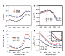
Although it exists at room temperature in an orthorhombic structure with space group Pnma, SnSe has been shown to undergo a transition to a structure with higher symmetry, space group Cmcm, at higher temperatures.[73] This structure consists of Sn-Se planes that are stacked upwards in the a-direction, which accounts for the poor performance out-of-plane (along a-axis). Upon transitioning to the Cmcm structure, SnSe maintains its low thermal conductivity but exhibits higher carrier mobilities, leading to its excellent ZT value.[71]
One particular impediment to further development of SnSe is that it has a relatively low carrier concentration: approximately 1017 cm−3. Further compounding this issue is the fact that SnSe has been reported to have low doping efficiency.[74]
However, such single crystalline materials suffer from inability to make useful devices due to their brittleness as well as narrow range of temperatures, where ZT is reported to be high. Further, polycrystalline materials made out of these compounds by several investigators have not confirmed the high ZT of these materials.
Production methods
Production methods for these materials can be divided into powder and crystal growth based techniques. Powder based techniques offer excellent ability to control and maintain desired carrier distribution, particle size, and composition.[75] In crystal growth techniques dopants are often mixed with melt, but diffusion from gaseous phase can also be used.[76] In the zone melting techniques disks of different materials are stacked on top of others and then materials are mixed with each other when a traveling heater causes melting. In powder techniques, either different powders are mixed with a varying ratio before melting or they are in different layers as a stack before pressing and melting.
There are applications, such as cooling of electronic circuits, where thin films are required. Therefore, thermoelectric materials can also be synthesized using physical vapor deposition techniques. Another reason to utilize these methods is to design these phases and provide guidance for bulk applications.
Significant improvement on 3D printing skills makes it possible for thermoelectric materials prepared from 3D printing inks, which are usually synthesized by dispersing inorganic powders to organic solvent or making a suspension.[77] Thermoelectric products are made from special materials that absorb heat and create electricity. The requirement of having complex geometries that fit in tightly constrained spaces, makes 3D printing the ideal manufacturing technique.[78] Also, printable materials that demonstrate good mechanical flexibility could be utilized for wearable thermoelectrics, which convert body energy to electricity.
Applications
Refrigeration
Thermoelectric materials can be used as refrigerators, called "thermoelectric coolers", or "Peltier coolers" after the Peltier effect that controls their operation. As a refrigeration technology, Peltier cooling is far less common than vapor-compression refrigeration. The main advantages of a Peltier cooler (compared to a vapor-compression refrigerator) are its lack of moving parts or refrigerant, and its small size and flexible shape (form factor).[79]
The main disadvantage of Peltier coolers is low efficiency. It is estimated that materials with ZT>3 (about 20–30% Carnot efficiency) would be required to replace traditional coolers in most applications.[57] Today, Peltier coolers are only used in niche applications, especially small scale, where efficiency is not important.[79]
Power generation
Thermoelectric efficiency depends on the figure of merit, ZT. There is no theoretical upper limit to ZT, and as ZT approaches infinity, the thermoelectric efficiency approaches the Carnot limit. However, no known thermoelectrics have a ZT>3.[80] As of 2010, thermoelectric generators serve application niches where efficiency and cost are less important than reliability, light weight, and small size.[81]
Internal combustion engines capture 20–25% of the energy released during fuel combustion.[82] Increasing the conversion rate can increase mileage and provide more electricity for on-board controls and creature comforts (stability controls, telematics, navigation systems, electronic braking, etc.)[83] It may be possible to shift energy draw from the engine (in certain cases) to the electrical load in the car, e.g., electrical power steering or electrical coolant pump operation.[82]
Cogeneration power plants use the heat produced during electricity generation for alternative purposes. Thermoelectrics may find applications in such systems or in solar thermal energy generation.[84]
See also
- Batteryless radio
- Pyroelectric effect
- Thermionic converter
References
- Snyder, G.J.; Toberer, E.S. (2008). "Complex Thermoelectric Materials". Nature Materials. 7 (2): 105–114. Bibcode:2008NatMa...7..105S. doi:10.1038/nmat2090. PMID 18219332.
- Wang, H; Pei, Y; LaLonde, AD; Snyder, GJ (2012). "Weak electron-phonon coupling contributing to high thermoelectric performance in n-type PbSe". Proc Natl Acad Sci U S A. 109 (25): 9705–9. Bibcode:2012PNAS..109.9705W. doi:10.1073/pnas.1111419109. PMC 3382475. PMID 22615358.
- Snyder, G.J. (2017). "Figure of merit ZT of a thermoelectric device defined from materials properties". Energy and Environmental Science. 10 (11): 2280–2283. doi:10.1039/C7EE02007D.
- Snyder, G.J. (2017). "Figure of merit ZT of a thermoelectric device defined from materials properties". Energy and Environmental Science. 10 (11): 2280–2283. doi:10.1039/C7EE02007D.
- Ioffe, A.F. (1960) Physics of semiconductors, Academic Press Inc., New York
- Kim, D.S.; Infante Ferreira, C.A. (2008). "Solar refrigeration options – a state-of-the-art review". International Journal of Refrigeration. 31: 3–15. doi:10.1016/j.ijrefrig.2007.07.011.
- Baranowski, L.L.; Toberer, E.S.; Snyder, GJ (2013). "The Misconception of Maximum Power and Power Factor in Thermoelectrics" (PDF). Journal of Applied Physics. 115: 126102. doi:10.1063/1.4869140.
- Timothy D. Sands (2005), Designing Nanocomposite Thermoelectric Materials
- Slack GA., in Rowe 2005
- Mahan, G. D. (1997). "Good Thermoelectrics". Solid State Physics - Advances in Research and Applications. Solid State Physics. 51. Academic Press. pp. 81–157. doi:10.1016/S0081-1947(08)60190-3. ISBN 9780126077513.
- Koumoto, Kunihito; Mori, Takao (2013-07-20). Thermoelectric Nanomaterials: Materials Design and Applications. Springer Science & Business Media. ISBN 9783642375378.
- Yanzhong, Pei; Heng, Wang; J., Snyder, G. (2012-12-04). "Band Engineering of Thermoelectric Materials". Advanced Materials. 24 (46): 6125–6135. doi:10.1002/adma.201202919. PMID 23074043. Retrieved 2015-10-23.
- Xing, Guangzong; Sun, Jifeng; Li, Yuwei; Fan, Xiaofeng; Zheng, Weitao; Singh, David J. (2017). "Electronic fitness function for screening semiconductors as thermoelectric materials". Physical Review Materials. 1 (6): 065405. arXiv:1708.04499. Bibcode:2017PhRvM...1f5405X. doi:10.1103/PhysRevMaterials.1.065405.
- Bhandari, C. M. in Rowe 2005, pp. 55–65
- Cava, R. J. (1990). "Structural chemistry and the local charge picture of copper-oxide superconductors". Science. 247 (4943): 656–62. Bibcode:1990Sci...247..656C. doi:10.1126/science.247.4943.656. PMID 17771881.
- Dresselhaus, M. S.; Chen, G.; Tang, M. Y.; Yang, R. G.; Lee, H.; Wang, D. Z.; Ren, Z. F.; Fleurial, J.-P.; Gogna, P. (2007). "New directions for low-dimensional thermoelectric materials" (PDF). Advanced Materials. 19 (8): 1043–1053. doi:10.1002/adma.200600527.
- Duck Young Chung; Hogan, T.; Schindler, J.; Iordarridis, L.; Brazis, P.; Kannewurf, C.R.; Baoxing Chen; Uher, C.; Kanatzidis, M.G. (1997). "Complex bismuth chalcogenides as thermoelectrics". XVI ICT '97. Proceedings ICT'97. 16th International Conference on Thermoelectrics (Cat. No.97TH8291). p. 459. doi:10.1109/ICT.1997.667185. ISBN 978-0-7803-4057-2.
- Venkatasubramanian, Rama; Siivola, Edward; Colpitts, Thomas; O'Quinn, Brooks (2001). "Thin-film thermoelectric devices with high room-temperature figures of merit". Nature. 413 (6856): 597–602. Bibcode:2001Natur.413..597V. doi:10.1038/35098012. PMID 11595940.
- Rowe 2005, Ch. 27.
- Heremans, J. P.; Jovovic, V.; Toberer, E. S.; Saramat, A.; Kurosaki, K.; Charoenphakdee, A.; Yamanaka, S.; Snyder, G. J. (2008). "Enhancement of Thermoelectric Efficiency in PbTe by Distortion of the Electronic Density of States" (PDF). Science. 321 (5888): 554–7. Bibcode:2008Sci...321..554H. doi:10.1126/science.1159725. PMID 18653890.
- Pei, Yanzhong; Lalonde, Aaron; Iwanaga, Shiho; Snyder, G. Jeffrey (2011). "High thermoelectric figure of merit in heavy hole dominated PbTe". Energy & Environmental Science. 4 (6): 2085. doi:10.1039/C0EE00456A.
- Pei, Yanzhong; Shi, Xiaoya; Lalonde, Aaron; Wang, Heng; Chen, Lidong; Snyder, G. Jeffrey (2011). "Convergence of electronic bands for high performance bulk thermoelectrics" (PDF). Nature. 473 (7345): 66–9. Bibcode:2011Natur.473...66P. doi:10.1038/nature09996. PMID 21544143.
- Quick, Darren (September 20, 2012). "World's most efficient thermoelectric material developed". Gizmag. Retrieved 16 December 2014.
- Biswas, K.; He, J.; Blum, I. D.; Wu, C. I.; Hogan, T. P.; Seidman, D. N.; Dravid, V. P.; Kanatzidis, M. G. (2012). "High-performance bulk thermoelectrics with all-scale hierarchical architectures". Nature. 489 (7416): 414–418. Bibcode:2012Natur.489..414B. doi:10.1038/nature11439. PMID 22996556.
- Rowe 2005, 32–33.
- Gatti, C., Bertini, L., Blake, N. P. and Iversen, B. B. (2003). "Guest–Framework Interaction in Type I Inorganic Clathrates with Promising Thermoelectric Properties: On the Ionic versus Neutral Nature of the Alkaline-Earth Metal Guest A in A8Ga16Ge30 (A=Sr, Ba)". Chemistry. 9 (18): 4556–68. doi:10.1002/chem.200304837. PMID 14502642.CS1 maint: multiple names: authors list (link)
- Rowe 2005, Ch. 32–33.
- Hirayama, Naomi; Iida, Tsutomu; Sakamoto, Mariko; Nishio, Keishi; Hamada, Noriaki (2019). "Substitutional and interstitial impurity p-type doping of thermoelectric Mg2Si: A theoretical study". Science and Technology of Advanced Materials. 20 (1): 160–172. doi:10.1080/14686996.2019.1580537. PMC 6419642. PMID 30891103.
- Khan, A.U.; Vlachos, N; Kyratsi, Th (2013). "High thermoelectric figure of merit of Mg2Si0.55-xSn0.4Ge0.05 materials doped with Bi and Sb". Scripta Materialia. 69 (8): 606–609. doi:10.1016/j.scriptamat.2013.07.008.
- Rowe 2005, Ch. 34.
- Nolas, G. S.; Slack, G. A.; Morelli, D. T.; Tritt, T. M.; Ehrlich, A. C. (1996). "The effect of rare-earth filling on the lattice thermal conductivity of skutterudites". Journal of Applied Physics. 79 (8): 4002. Bibcode:1996JAP....79.4002N. doi:10.1063/1.361828.
- Khan, Atta U.; Kobayashi, Kazuaki; Tang, Dai-Ming; Yamauchi, Yasuke; Hasegawa, Kotone; Mitome, Masanori; Xue, Yanming; Jiang, Baozhen; Tsuchiay, Koichi; Dmitri, Golberg; Mori, Takao (2017). "Nano-micro-porous skutterudites with 100% enhancement in ZT for high performance thermoelectricity". Nano Energy. 31: 152–159. doi:10.1016/j.nanoen.2016.11.016.
- "Spacecraft 'Nuclear Batteries' Could Get a Boost from New Materials". JPL News. Jet Propulsion Laboratory. 13 October 2016.
- Rowe 2005, Ch. 35.
- Ohtaki, Michitaka (2011). "Recent aspects of oxide thermoelectric materials for power generation from mid-to-high temperature heat source". Journal of the Ceramic Society of Japan. 119 (1395): 770–775. doi:10.2109/jcersj2.119.770.
- Matsuno, Jobu; Fujioka, Jun; Okuda, Tetsuji; Ueno, Kazunori; Mizokawa, Takashi; Katsufuji, Takuro (2018). "Strongly correlated oxides for energy harvesting". Science and Technology of Advanced Materials. 19 (1): 899–908. Bibcode:2018STAdM..19..899M. doi:10.1080/14686996.2018.1529524. PMC 6454405. PMID 31001365.
- Music, D.; Schneider, J.M. (2015). "Critical evaluation of the colossal Seebeck coefficient of nanostructured rutile MnO2". Journal of Physics: Condensed Matter. 27 (11): 115302. Bibcode:2015JPCM...27k5302M. doi:10.1088/0953-8984/27/11/115302. PMID 25730181.
- Music, D.; Chen, Y.-T.; Bliem, P.; Geyer, R.W. (2015). "Amorphous-crystalline transition in thermoelectric NbO2". Journal of Physics D: Applied Physics. 48 (27): 275301. Bibcode:2015JPhD...48.5301M. doi:10.1088/0022-3727/48/27/275301.
- Onozato, T.; Katase, T.; Yamamoto, A.; et al. (2016). "Optoelectronic properties of valence-state-controlled amorphous niobium oxide". Journal of Physics: Condensed Matter. 28 (25): 255001. Bibcode:2016JPCM...28y5001O. doi:10.1088/0953-8984/28/25/255001. PMID 27168317.
- Huang, Lihong; Zhang, Qinyong; Yuan, Bo; Lai, Xiang; Yan, Xiao; Ren, Zhifeng (2016). "Recent progress in half-Heusler thermoelectric materials". Materials Research Bulletin. 76: 107–112. doi:10.1016/j.materresbull.2015.11.032.
- Yan, Xiao; Joshi, Giri; Liu, Weishu; Lan, Yucheng; Wang, Hui; Lee, Sangyeop; Simonson, J. W.; Poon, S. J.; Tritt, T. M.; Chen, Gang; Ren, Z. F. (2011). "Enhanced Thermoelectric Figure of Merit of p-Type Half-Heuslers". Nano Letters. 11 (2): 556–560. Bibcode:2011NanoL..11..556Y. doi:10.1021/nl104138t. PMID 21186782.
- Kimura, Yoshisato; Ueno, Hazuki; Mishima, Yoshinao (2009). "Thermoelectric Properties of Directionally Solidified Half-Heusler (Ma0.5,Mb0.5)NiSn (Ma, Mb = Hf, Zr, Ti) Alloys". Journal of Electronic Materials. 38 (7): 934–939. doi:10.1007/s11664-009-0710-x.
- Petsagkourakis, Ioannis; Tybrandt, Klas; Crispin, Xavier; Ohkubo, Isao; Satoh, Norifusa; Mori, Takao (2018). "Thermoelectric materials and applications for energy harvesting power generation". Science and Technology of Advanced Materials. 19 (1): 836–862. Bibcode:2018STAdM..19..836P. doi:10.1080/14686996.2018.1530938. PMC 6454408. PMID 31001364.
- Zhan, Tianzhuo; Yamato, Ryo; Hashimoto, Shuichiro; Tomita, Motohiro; Oba, Shunsuke; Himeda, Yuya; Mesaki, Kohei; Takezawa, Hiroki; Yokogawa, Ryo; Xu, Yibin; Matsukawa, Takashi; Ogura, Atsushi; Kamakura, Yoshinari; Watanabe, Takanobu (2018). "Miniaturized planar Si-nanowire micro-thermoelectric generator using exuded thermal field for power generation". Science and Technology of Advanced Materials. 19 (1): 443–453. Bibcode:2018STAdM..19..443Z. doi:10.1080/14686996.2018.1460177. PMC 5974757. PMID 29868148.
- Nakamura, Yoshiaki (2018). "Nanostructure design for drastic reduction of thermal conductivity while preserving high electrical conductivity". Science and Technology of Advanced Materials. 19 (1): 31–43. Bibcode:2018STAdM..19...31N. doi:10.1080/14686996.2017.1413918. PMC 5769778. PMID 29371907.
- Kandemir, Ali; Ozden, Ayberk; Cagin, Tahir; Sevik, Cem (2017). "Thermal conductivity engineering of bulk and one-dimensional Si-Ge nanoarchitectures". Science and Technology of Advanced Materials. 18 (1): 187–196. Bibcode:2017STAdM..18..187K. doi:10.1080/14686996.2017.1288065. PMC 5404179. PMID 28469733.
- "Improved thermoelectric materials may give a push to Moore's law". KurzweilAI. September 2, 2013.
- Voneshen, D. J.; Refson, K.; Borissenko, E.; Krisch, M.; Bosak, A.; Piovano, A.; Cemal, E.; Enderle, M.; Gutmann, M. J.; Hoesch, M.; Roger, M.; Gannon, L.; Boothroyd, A. T.; Uthayakumar, S.; Porter, D. G.; Goff, J. P. (2013). "Suppression of thermal conductivity by rattling modes in thermoelectric sodium cobaltate" (PDF). Nature Materials. 12 (11): 1028–1032. Bibcode:2013NatMa..12.1028V. doi:10.1038/nmat3739. PMID 23975057.
- Nolas, G.S.; Goldsmid, H.J. (2002). "The figure of merit in amorphous thermoelectrics". Physica Status Solidi A. 194 (1): 271–276. Bibcode:2002PSSAR.194..271N. doi:10.1002/1521-396X(200211)194:1<271::AID-PSSA271>3.0.CO;2-T.
- Goncalves, A.P.; Lopes, E.B.; Rouleau, O.; Godart, C. (2010). "Conducting glasses as new potential thermoelectric materials: the Cu-Ge-Te case". Journal of Materials Chemistry. 20 (8): 1516–1521. doi:10.1039/B908579C.
- Music, D.; Geyer, R.W.; Hans, M. (2016). "High-throughput exploration of thermoelectric and mechanical properties of amorphous NbO2 with transition metal additions". Journal of Applied Physics. 120 (4): 045104. Bibcode:2016JAP...120d5104M. doi:10.1063/1.4959608.
- Fujimoto, Y.; Uenuma, M.; Ishikawa, Y.; Uraoka, Y. (2015). "Analysis of thermoelectric properties of amorphous InGaZnO thin film by controlling carrier concentration". AIP Advances. 5 (9): 097209. Bibcode:2015AIPA....5i7209F. doi:10.1063/1.4931951.
- Zhou, Y.; Tan, Q.; Zhu, J.; Li, S.; Liu, C.; Lei, Y.; Li, L. (2015). "Thermoelectric properties of amorphous Zr-Ni-Sn thin films deposited by magnetron sputtering". Journal of Electronic Materials. 44 (6): 1957–1962. Bibcode:2015JEMat..44.1957Z. doi:10.1007/s11664-014-3610-7.
- Takiguchi, H.; Yoshikawa, Z.; Miyazaki, H.; Okamoto, Y.; Morimoto, J. (2010). "The Role of Au in the Thermoelectric Properties of Amorphous Ge/Au and Si/Au Thin Films". Journal of Electronic Materials. 39 (9): 1627–1633. Bibcode:2010JEMat..39.1627T. doi:10.1007/s11664-010-1267-4.
- Ramesh, K. V; Sastry, D. L (2007). "DC electrical conductivity, thermoelectric power measurements of TiO2-substituted lead vanadate glasses". Physica B. 387 (1–2): 45–51. Bibcode:2007PhyB..387...45R. doi:10.1016/j.physb.2006.03.026.
- Rowe 2005, Ch. 38.
- Harman, T. C.; Taylor, PJ; Walsh, MP; Laforge, BE (2002). "Quantum dot superlattice thermoelectric materials and devices" (PDF). Science. 297 (5590): 2229–32. Bibcode:2002Sci...297.2229H. doi:10.1126/science.1072886. PMID 12351781.
- Rowe 2005, Ch. 40.
- Rowe 2005, Ch. 41.
- Anno, Yuki; Imakita, Yuki; Takei, Kuniharu; Akita, Seiji; Arie, Takayuki (2017). "Enhancement of graphene thermoelectric performance through defect engineering". 2D Materials. 4 (2): 025019. Bibcode:2017TDM.....4b5019A. doi:10.1088/2053-1583/aa57fc.
- Mu, X.; Wu, X.; Zhang, T.; Go, D. B.; Luo, T. (2014). "Thermal transport in graphene oxide—from ballistic extreme to amorphous limit". Scientific Reports. 4: 3909. Bibcode:2014NatSR...4E3909M. doi:10.1038/srep03909. PMC 3904152. PMID 24468660.
- Anno, Yuki; Takei, Kuniharu; Akita, Seiji; Arie, Takayuki (2014). "Artificially controlled synthesis of graphene intramolecular heterojunctions for phonon engineering". Physica Status Solidi RRL. 8 (8): 692–697. Bibcode:2014PSSRR...8..692A. doi:10.1002/pssr.201409210.
- Chen, Shanshan; Li, Qiongyu; Zhang, Qimin; Qu, Yan; Ji, Hengxing; Ruoff, Rodney S; Cai, Weiwei (2012). "Thermal conductivity measurements of suspended graphene with and without wrinkles by micro-Raman mapping". Nanotechnology. 23 (36): 365701. Bibcode:2012Nanot..23J5701C. doi:10.1088/0957-4484/23/36/365701. PMID 22910228.
- Rowe 2005, Ch. 16, 39.
- Rowe 2005, Ch. 39.
- Rowe 2005, Ch. 49.
- Minnich, A. J.; Dresselhaus, M. S.; Ren, Z. F.; Chen, G. (2009). "Bulk nanostructured thermoelectric materials: current research and future prospects". Energy & Environmental Science. 2 (5): 466. doi:10.1039/b822664b.
- Biswas, Kanishka; He, Jiaqing; Zhang, Qichun; Wang, Guoyu; Uher, Ctirad; Dravid, Vinayak P.; Kanatzidis, Mercouri G. (2011). "Strained endotaxial nanostructure with high thermoelectric figure of merit". Nature Chemistry. 3 (2): 160–6. Bibcode:2011NatCh...3..160B. doi:10.1038/nchem.955. PMID 21258390.
- Zhao, Li-Dong; Lo, Shih-Han; Zhang, Yongsheng; Sun, Hui; Tan, Gangjian; Uher, Ctirad; Wolverton, C.; Dravid, Vinayak P.; Kanatzidis, Mercouri G. (2014). "Ultralow thermal conductivity and high thermoelectric figure of merit in SnSe crystals". Nature. 508 (7496): 373–7. Bibcode:2014Natur.508..373Z. doi:10.1038/nature13184. PMID 24740068.
- Zhang, H.; Talapin, D. V. (2014). "Thermoelectric Tin Selenide: The Beauty of Simplicity". Angew. Chem. Int. Ed. 53 (35): 9126–9127. doi:10.1002/anie.201405683. PMID 25044424.
- Zhao, L-D.; Lo, S-H.; Zhang, Y.; Sun, H.; Tan, G.; Uher, C.; Wolverton, C.; Dravid, V.; Kanatzidis, M. (2014). "Ultralow thermal conductivity and high thermoelectric figure of merit in SnSe crystals". Nature. 508 (7496): 373–377. Bibcode:2014Natur.508..373Z. doi:10.1038/nature13184. PMID 24740068.
- Zhao, Li-Dong; Lo, Shih-Han; Zhang, Yongsheng; Sun, Hui; Tan, Gangjian; Uher, Ctirad; Wolverton, C.; Dravid, Vinayak P.; Kanatzidis, Mercouri G. (2014). "Ultralow thermal conductivity and high thermoelectric figure of merit in Sn Se crystals". Nature. 508 (7496): 373–377. Bibcode:2014Natur.508..373Z. doi:10.1038/nature13184. PMID 24740068.
- Bernardes-Silva, Ana Cláudia; Mesquita, A.F.; Neto, E. de Moura; Porto, A.O.; Ardisson, J.D.; Lima, G.M. de; Lameiras, F.S. (2005). "XRD and 119Sn Mossbauer spectroscopy characterization of SnSe obtained from a simple chemical route". Materials Research Bulletin. 40 (9): 1497–1505. doi:10.1016/j.materresbull.2005.04.021.
- Chen, C-L.; Wang, H.; Chen, Y-Y.; Daya, T.; Snyder, G. J. (2014). "Thermoelectric properties of p-type polycrystalline SnSe doped with Ag". J. Mater. Chem. A. 2 (29): 11171. doi:10.1039/c4ta01643b.
- Yazdani, Sajad; Pettes, Michael Thompson (2018-10-26). "Nanoscale self-assembly of thermoelectric materials: a review of chemistry-based approaches". Nanotechnology. 29 (43): 432001. Bibcode:2018Nanot..29Q2001Y. doi:10.1088/1361-6528/aad673. ISSN 0957-4484. PMID 30052199.
- He, Jian; Tritt, Terry M. (2017-09-29). "Advances in thermoelectric materials research: Looking back and moving forward". Science. 357 (6358): eaak9997. doi:10.1126/science.aak9997. ISSN 0036-8075. PMID 28963228.
- Kim, Fredrick; Kwon, Beomjin; Eom, Youngho; Lee, Ji Eun; Park, Sangmin; Jo, Seungki; Park, Sung Hoon; Kim, Bong-Seo; Im, Hye Jin (2018). "3D printing of shape-conformable thermoelectric materials using all-inorganic Bi2Te3-based inks". Nature Energy. 3 (4): 301–309. Bibcode:2018NatEn...3..301K. doi:10.1038/s41560-017-0071-2.
- Wang, Liming; Zhang, Zimeng; Geng, Linxiao; Yuan, Tianyu; Liu, Yuchen; Guo, Juchen; Fang, Lei; Qiu, Jingjing; Wang, Shiren (2018). "Solution-printable fullerene/TiS2 organic/inorganic hybrids for high-performance flexible n-type thermoelectrics". Energy & Environmental Science. 11 (5): 1307–1317. doi:10.1039/c7ee03617e.
- Champier, Daniel (2017). "Thermoelectric generators: A review of applications". Energy Conversion and Management. 140: 162–181. doi:10.1016/j.enconman.2017.02.070.
- Tritt, Terry M.; Subramanian, M. A. (2011). "Thermoelectric Materials, Phenomena, and Applications: A Bird's Eye View" (PDF). MRS Bulletin. 31 (3): 188–198. doi:10.1557/mrs2006.44.
- Labudovic, M.; Li, J. (2004). "Modeling of TE cooling of pump lasers". IEEE Transactions on Components and Packaging Technologies. 27 (4): 724–730. doi:10.1109/TCAPT.2004.838874.
- Yang, J. (2005). "Potential applications of thermoelectric waste heat recovery in the automotive industry". ICT 2005. 24th International Conference on Thermoelectrics, 2005. p. 170. doi:10.1109/ICT.2005.1519911. ISBN 978-0-7803-9552-7.
- Fairbanks, J. (2006-08-24) Thermoelectric Developments for Vehicular Applications, U.S. Department of Energy: Energy Efficiency and Renewable Energy.
- Goldsmid, H.J.; Giutronich, J.E.; Kaila, M.M. (1980). "Thermoelectrics: Direct Solar Thermal Energy Conversion" (PDF). Solar Energy. 24 (5): 435–440. Bibcode:1980SoEn...24..435G. doi:10.1016/0038-092X(80)90311-4.
Bibliography
- Rowe, D.M. (2018-10-03). Thermoelectrics Handbook: Macro to Nano. CRC Press. ISBN 978-1-4200-3890-3.CS1 maint: ref=harv (link)