Scanning gate microscopy
Scanning gate microscopy (SGM) is a scanning probe microscopy technique with an electrically conductive tip used as a movable gate that couples capacitively to the sample and probes electrical transport on the nanometer scale.[1][2] Typical samples are mesoscopic devices, often based on semiconductor heterostructures, such as quantum point contacts or quantum dots. Carbon nanotubes too have been investigated.
Operating principle
In SGM one measures the sample's electrical conductance as a function of tip position and tip potential. This is in contrast to other microscopy techniques where the tip is used as a sensor, e.g., for forces.
Development
SGMs were developed in the late 1990s from atomic force microscopes. Most importantly, these had to be adapted for use at low temperatures, often 4 kelvins or less, as the samples under study do not work at higher temperatures. Today an estimated number of ten research groups worldwide use the technique.
References
- Sellier, H; Hackens, B; Pala, M G; Martins, F; Baltazar, S; Wallart, X; Desplanque, L; Bayot, V; Huant, S (2011). "On the imaging of electron transport in semiconductor quantum structures by scanning-gate microscopy: successes and limitations". Semiconductor Science and Technology. 26 (6): 064008. arXiv:1104.2032. Bibcode:2011SeScT..26f4008S. doi:10.1088/0268-1242/26/6/064008. ISSN 0268-1242.
- Gorini, Cosimo; Jalabert, Rodolfo A.; Szewc, Wojciech; Tomsovic, Steven; Weinmann, Dietmar (2013). "Theory of scanning gate microscopy". Physical Review B. 88 (3). arXiv:1302.1151. Bibcode:2013PhRvB..88c5406G. doi:10.1103/PhysRevB.88.035406. ISSN 1098-0121.
| Common | 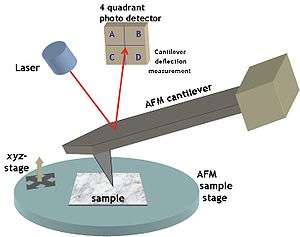 Typical atomic force microscopy set-up | |
|---|---|---|
| Other |
| |
| Applications | ||
| See also | ||