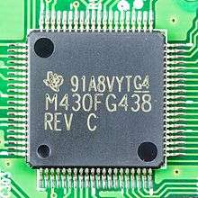
TI MSP430
The MSP430 is a mixed-signal microcontroller family from Texas Instruments. Built around a 16-bit CPU, the MSP430 is designed for low cost and, specifically, low power consumption[1] embedded applications.
| Designer | Texas Instruments |
|---|---|
| Bits | 16-bit |
| Type | Memory-Memory |
| Registers | |
| 16, R0 – Program Counter, R1 – Stack Pointer, R2 – Status Register, R2/R3 – Constant Generator | |
Applications
The MSP430 can be used for low powered embedded devices. The current drawn in idle mode can be less than 1 µA. The top CPU speed is 25 MHz. It can be throttled back for lower power consumption. The MSP430 also uses six different low-power modes, which can disable unneeded clocks and CPU. Additionally, the MSP430 is capable of wake-up times below 1 microsecond, allowing the microcontroller to stay in sleep mode longer, minimizing its average current consumption. The device comes in a variety of configurations featuring the usual peripherals: internal oscillator, timer including PWM, watchdog, USART, SPI, I²C, 10/12/14/16/24-bit ADCs, and brownout reset circuitry. Some less usual peripheral options include comparators (that can be used with the timers to do simple ADC), on-chip op-amps for signal conditioning, 12-bit DAC, LCD driver, hardware multiplier, USB, and DMA for ADC results. Apart from some older EPROM (MSP430E3xx) and high volume mask ROM (MSP430Cxxx) versions, all of the devices are in-system programmable via JTAG (full four-wire or Spy-Bi-Wire) or a built in bootstrap loader (BSL) using UART such as RS232, or USB on devices with USB support.
There are, however, limitations that preclude its use in more complex embedded systems. The MSP430 does not have an external memory bus, so it is limited to on-chip memory (up to 512 KB flash memory and 66 KB RAM) which may be too small for applications that require large buffers or data tables. Also, although it has a DMA controller, it is very difficult to use it to move data off the chip due to a lack of a DMA output strobe.[2]
MSP430 part numbering
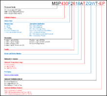
An MSP430 part number such as "MSP430F2618ATZQWT-EP" consists of the following pieces:
- MSP430: Standard prefix.
- F: Indicates a memory type or specialized application. "F" indicating flash memory is by far the most popular. Other options for memory type include "C" for masked ROM, "FR" for FRAM, "G" for Flash Value Line, and "L" as in the MSP430L09x series, which indicates a RAM-only part; it must remain continuously powered to retain its programming. A second letter (except for "FR") indicates a specialized application for the part. For example, "G" is an optional specialization letter indicating hardware support for a specialized use. "E" indicates special electricity meter functions, "G" devices are designed for medical instrumentation, and "W" devices include a special "scan interface" designed for flow meters. An exception is the MSP430FG2xx devices, which are considered a separate generation.
- 2: The generation of device. There can be significant changes to core peripherals (clock generators, UARTs, etc.) in different generations. These are not in chronological order, but rather higher values roughly indicate greater size, complexity and cost. For example, generations 3 and 4 include LCD controllers which the others do not.
- 6: The model within the generation. This indicates the mixture of on-board peripheral devices and number of pins.
- 18: One or two digits indicating the amount of memory on the device. The numbering is (mostly) consistent throughout the MSP430 series. Not all suffixes are valid with all models; most models are available in 3–6 memory sizes, chosen to match the other capabilities of the device. Larger numbers indicate increasing amounts of memory, but sometimes one type of memory (RAM or ROM) is sacrificed to fit more of the other.
| Suffix | RAM | ROM | Suffix | RAM | ROM | |
|---|---|---|---|---|---|---|
| 0 | 128 | 1 K | 10 | 5 K | 32 K | |
| 1 | 128 | 2 K | 11 | 10 K | 48 K | |
| 2 | 256 | 4 K | 12 | 5 K | 55/56 K | |
| 3 | 256 | 8 K | 13 | |||
| 4 | 512 | 12 K | 14 | |||
| 5 | 512 | 16 K | 15 | |||
| 6 | 1 K | 24 K | 16 | 4 K | 92 K | |
| 7 | 1 K | 32 K | 17 | 8 K | 92 K | |
| 8 | 2 K | 48K | 18 | 8 K | 116 K | |
| 9 | 2 K | 60K | 19 | 4 K | 120 K | |
- An optional suffix digit indicating a variant device, adding or deleting some analog peripherals. For example, a "1" suffix may indicate the addition of a comparator or deletion of an ADC. If the memory size is "1", this suffix can be confused with part of the memory size, but no single model is available in both "1" and "10" (or greater) memory sizes.
- An optional "A" suffix indicating an upward-compatible revised version. The MSP430F11x1A has an additional 256 bytes of data flash not present in the plain 'F11x1.
Trailing suffix letters indicate options not visible to software:
- T: Indicates a temperature range of −40 °C to +105 °C.
- ZQW: Indicates the package the part is kept in. "ZQW" is a TI-specific name for a ball grid array.
- T: Indicates that the parts are shipped in small reel (7-inch) packaging.
- -EP: Indicates an additional feature. "-Q1" specifies that the part is automotive qualified. "-EP" and "-HT" indicate extended temperature products. Enhanced products, "-EP", have a temperature range from -40 °C to 125 °C, and extreme temperature parts, "-HT", have a temperature range from -56 °C to 150 °C.
MSP430 generations
There are six general generations of MSP430 processors. In order of development, they are the '3xx generation, the '1xx generation, the '4xx generation, the '2xx generation, the '5xx generation, and the '6xx generation. The digit after the generation identifies the model (generally higher model numbers are larger and more capable), the third digit identifies the amount of memory on board, and the fourth, if present, identifies a minor model variant. The most common variation is a different on-chip analog-to-digital converter.
The 3xx and 1xx generations are limited to a 16-bit address space. In the later generations this was expanded to include '430X' instructions that allow a 20-bit address space. As happened with other processor architectures (e.g. the processor of the PDP-11), extending the addressing range beyond the 16-bit word size introduced some peculiarities and inefficiencies for programs larger than 64 kBytes.
In the following list, it helps to think of the typical 200 mA·Hr capacity of a CR2032 lithium coin cell as 200,000 μA·Hr, or 22.8 μA·year. Thus, considering only the CPU draw, such a battery could supply a 0.7 μA current draw for 32 years. (In reality, battery self-discharge would reduce this number.)
The significance of the 'RAM retention' vs the 'real-time clock mode' is that in real time clock mode the CPU can go to sleep with a clock running which will wake it up at a specific future time. In RAM retention mode, some external signal is required to wake it, e.g. I/O pin signal or SPI slave receive interrupt.
MSP430x1xx series
The MSP430x1xx Series is the basic generation without an embedded LCD controller. They are generally smaller than the '3xx generation. These flash- or ROM-based ultra-low-power MCUs offer 8 MIPS, 1.8–3.6 V operation, up to 60 KB flash, and a wide range of analog and digital peripherals.
- Power specification overview, as low as:
- 0.1 μA RAM retention
- 0.7 μA real-time clock mode
- 200 μA / MIPS active
- Features fast wake-up from standby mode in less than 6 µs.
- Power specification overview, as low as:
- Device parameters
- Flash options: 1–60 KB
- ROM options: 1–16 KB
- RAM : 128 B–10 KB
- GPIO options: 14, 22, 48 pins
- ADC options: Slope, 10 & 12-bit SAR
- Other integrated peripherals: 12-bit DAC, up to 2 16-bit timers, watchdog timer, brown-out reset, SVS, USART module (UART, SPI), DMA, 16×16 multiplier, Comparator_A, temperature sensor
- Device parameters
MSP430F2xx series
The MSP430F2xx Series are similar to the '1xx generation, but operate at even lower power, support up to 16 MHz operation, and have a more accurate (±2%) on-chip clock that makes it easier to operate without an external crystal. These flash-based ultra-low power devices offer 1.8–3.6 V operation. Includes the very-low power oscillator (VLO), internal pull-up/pull-down resistors, and low-pin count options.
- Power specification overview, as low as:
- 0.1 μA RAM retention
- 0.3 μA standby mode (VLO)
- 0.7 μA real-time clock mode
- 220 μA / MIPS active
- Feature ultra-fast wake-up from standby mode in less than 1 μs
- Power specification overview, as low as:
- Device parameters
- Flash options: 1–120 KB
- RAM options: 128 B – 8 KB
- GPIO options: 10, 11, 16, 24, 32, and 48 pins
- ADC options: Slope, 10 & 12-bit SAR, 16 & 24-bit Sigma Delta
- Other integrated peripherals: operational amplifiers, 12-bit DAC, up to 2 16-bit timers, watchdog timer, brown-out reset, SVS, USI module (I²C, SPI), USCI module, DMA, 16×16 multiplier, Comparator_A+, temperature sensor
- Device parameters
MSP430G2xx series
The MSP430G2xx Value Series features flash-based Ultra-Low Power MCUs up to 16 MIPS with 1.8–3.6 V operation. Includes the Very-Low power Oscillator (VLO), internal pull-up/pull-down resistors, and low-pin count options, at lower prices than the MSP430F2xx series.
- Ultra-Low Power, as low as (@2.2 V):
- 0.1 μA RAM retention
- 0.4 μA Standby mode (VLO)
- 0.7 μA real-time clock mode
- 220 μA / MIPS active
- Ultra-Fast Wake-Up From Standby Mode in <1 μs
- Ultra-Low Power, as low as (@2.2 V):
- Device parameters
- Flash options: 0.5–56 KB
- RAM options: 128 B–4 KB
- GPIO options: 10, 16, 24, 32 pins
- ADC options: Slope, 10-bit SAR
- Other integrated peripherals: Capacitive Touch I/O, up to 3 16-bit timers, watchdog timer, brown-out reset, USI module (I²C, SPI), USCI module, Comparator_A+, Temp sensor
- Device parameters
MSP430x3xx series
The MSP430x3xx Series is the oldest generation, designed for portable instrumentation with an embedded LCD controller. This also includes a frequency-locked loop oscillator that can automatically synchronize to a low-speed (32 kHz) crystal. This generation does not support EEPROM memory, only mask ROM and UV-eraseable and one-time programmable EPROM. Later generations provide only flash memory and mask ROM options. These devices offer 2.5–5.5 V operation, up to 32 KB ROM.
- Power specification overview, as low as:
- 0.1 μA RAM retention
- 0.9 μA real-time clock mode
- 160 μA / MIPS active
- Features fast wake-up from standby mode in less than 6 µs.
- Power specification overview, as low as:
- Device parameters:
- ROM options: 2–32 KB
- RAM options: 512 B–1 KB
- GPIO options: 14, 40 pins
- ADC options: Slope, 14-bit SAR
- Other integrated peripherals: LCD controller, multiplier
- Device parameters:
MSP430x4xx series
The MSP430x4xx Series are similar to the '3xx generation, but include an integrated LCD controller, and are larger and more capable. These flash or ROM based devices offers 8–16 MIPS at 1.8–3.6 V operation, with FLL, and SVS. Ideal for low power metering and medical applications.
- Power specification overview, as low as:
- 0.1 μA RAM retention
- 0.7 μA real-time clock mode
- 200 μA / MIPS active
- Features fast wake-up from standby mode in less than 6 µs.
- Power specification overview, as low as:
- Device parameters:
- Flash/ROM options: 4 – 120 KB
- RAM options: 256 B – 8 KB
- GPIO options: 14, 32, 48, 56, 68, 72, 80 pins
- ADC options: Slope, 10 & 12-bit SAR, 16-bit Sigma Delta
- Other integrated peripherals: SCAN_IF, ESP430, 12-bit DAC, Op Amps, RTC, up to 2 16-bit timers, watchdog timer, basic timer, brown-out reset, SVS, USART module (UART, SPI), USCI module, LCD Controller, DMA, 16×16 & 32x32 multiplier, Comparator_A, temperature sensor, 8 MIPS CPU Speed
- Device parameters:
MSP430x5xx series
The MSP430x5xx Series are able to run up to 25 MHz, have up to 512 KB flash memory and up to 66 KB RAM. This flash-based family features low active power consumption with up to 25 MIPS at 1.8–3.6 V operation (165 uA/MIPS). Includes an innovative power management module for optimal power consumption and integrated USB.[3]
- Power specification overview, as low as:
- 0.1 μA RAM retention
- 2.5 μA real-time clock mode
- 165 μA / MIPS active
- Features fast wake-up from standby mode in less than 5 µs.
- Power specification overview, as low as:
- Device parameters:
- Flash options: up to 512 KB
- RAM options: up to 66 KB
- ADC options: 10 & 12-bit SAR
- GPIO options: 29, 31, 47, 48, 63, 67, 74, 87 pins
- Other integrated peripherals: High resolution PWM, 5 V I/O's, USB, backup battery switch, up to 4 16-bit timers, watchdog timer, Real-Time Clock, brown-out reset, SVS, USCI module, DMA, 32x32 multiplier, Comp B, temperature sensor
- Device parameters:
MSP430x6xx series
The MSP430x6xx Series are able to run up to 25 MHz, have up to 512 KB flash memory and up to 66 KB RAM. This flash-based family features low active power consumption with up to 25 MIPS at 1.8–3.6 V operation (165 uA/MIPS). Includes an innovative power management module for optimal power consumption and integrated USB.
- Power specification overview, as low as:
- 0.1 μA RAM retention
- 2.5 μA real-time clock mode
- 165 μA / MIPS active
- Features fast wake-up from standby mode in less than 5 µs.
- Power specification overview, as low as:
- Device parameters:
- Flash options: up to 512 KB
- RAM options: up to 66 KB
- ADC options: 12-bit SAR
- GPIO options: 74 pins
- Other integrated peripherals: USB, LCD, DAC, Comparator_B, DMA, 32x32 multiplier, power management module (BOR, SVS, SVM, LDO), watchdog timer, RTC, Temp sensor
- Device parameters:
RF SoC (CC430) series
The RF SoC (CC430) Series provides tight integration between the microcontroller core, peripherals, software, and RF transceiver. Features <1 GHz RF transceiver, with 1.8 V–3.6 V operation. Programming using Arduino IDE is possible via the panStamp API.
- Power specification overview, as low as:
- 1 μA RAM retention
- 1.7 μA real-time clock mode
- 180 μA / MIPS active
- Power specification overview, as low as:
- Device parameters:
- Speed options: up to 20 MHz
- Flash options: up to 32 KB
- RAM options: up to 4 KB
- ADC options: 12-bit SAR
- GPIO options: 30 & 44 pins
- Other integrated peripherals: LCD Controller, up to 2 16-bit timers, watchdog timer, RTC, power management module (BOR, SVS, SVM, LDO), USCI module, DMA, 32x32 multiplier, Comp B, temperature sensor
- Device parameters:
FRAM series
The FRAM Series from Texas Instruments provides unified memory with dynamic partitioning and memory access speeds 100 times faster than flash. FRAM is also capable of zero power state retention in all power modes, which means that writes are guaranteed, even in the event of a power loss. With a write endurance of over 100 trillion cycles, EEPROM is no longer required. Active power consumption at less than 100μA/MHz.
- Power specification overview, as low as:
- 320 nA RAM retention
- 0.35 μA real-time clock mode
- 82 μA / MIPS active
- Power specification overview, as low as:
- Device parameters:
- Speed options: 8 to 24 MHz
- FRAM options: 4 to 256 KB
- RAM options: 0.5 to 8 KB
- ADC options: 10 or 12-bit SAR
- GPIO options: 17 to 83 GPIO pins
- Other possible integrated peripherals: MPU, up to 6 16-bit timers, watchdog timer, RTC, power management module (BOR, SVS, SVM, LDO), USCI module, DMA, multiplier, Comp B, temperature sensor, LCD driver, I2C and UART BSL, Extended Scan Interface, 32 bit multiplier, AES, CRC, signal processing acceleration, capacitive touch, IR modulation
- Device parameters:
Low voltage series
The Low Voltage Series include the MSP430C09x and MSP430L092 parts. These 2 series of low voltage 16 bit microcontrollers have configurations with two 16-bit timers, an 8-bit analog-to-digital (A/D) converter, an 8-bit digital-to-analog (D/A) converter, and up to 11 I/O pins.
- Power specification overview, as low as:
- 1 μA RAM retention
- 1.7 μA real-time clock mode
- 180 μA / MIPS active
- Power specification overview, as low as:
- Device parameters:
- Speed options: 4 MHz
- ROM options: 1–2 kB
- SRAM options: 2 kB
- ADC options: 8-bit SAR
- GPIO options: 11 pins
- Other integrated peripherals: up to 2 16-bit timers, watchdog timer, brown-out reset, SVS, comparator, temperature sensor
- Device parameters:
Other MSP430 families
Additional families within MSP430 include Fixed Function, Automotive, and Extended Temp parts.
Fixed Function: The MSP430BQ1010 16-bit microcontroller is an advanced fixed-function device that forms the control and communications unit on the receiver side for wireless power transfer in portable applications. MSP430BQ1010 complies with the Wireless Power Consortium (WPC) specification. For more information, see Contactless Power.
Automotive: Automotive MSP430 microcontrollers (MCUs) from Texas Instruments (TI) are 16-bit, RISC-based, mixed-signal processors that are AEC-Q100 qualified and suitable for automotive applications in environments up to 105 °C ambient temperature. LIN compliant drivers for the MSP430 MCU provided by IHR GmbH.
Extended Temp: MSP430 devices are very popular in harsh environments such as industrial sensing for their low power consumption and innovative analog integration. Some harsh environment applications include transportation/automotive, renewable energy, military/space/avionics, mineral exploration, industrial, and safety & security.
- Device Definitions:
- HT: -55 °C to 150 °C
- EP: Enhanced products -55 °C to 125 °C
- Q1: Automotive Q100 qualified -40 °C to 105 °C
- T: Extended temperature -40 °C to 105 °C applications
- Device Definitions:
Note that when the flash size is over 64K words (128 KBytes), instruction addresses can no longer be encoded in just two bytes. This change in pointer size causes some incompatibilities with previous parts.
Peripherals
The MSP430 peripherals are generally easy to use, with (mostly) consistent addresses between models, and no write-only registers (except for the hardware multiplier).
General purpose I/O ports 0–10
If the peripheral is not needed, the pin may be used for general purpose I/O. The pins are divided into 8-bit groups called "ports", each of which is controlled by a number of 8-bit registers. In some cases, the ports are arranged in pairs which can be accessed as 16-bit registers.
The MSP430 family defines 11 I/O ports, P0 through P10, although no chip implements more than 10 of them. P0 is only implemented on the '3xx family. P7 through P10 are only implemented on the largest members (and highest pin count versions) of the '4xx and '2xx families. The newest '5xx and '6xx families has P1 through P11, and the control registers are reassigned to provide more port pairs. Each port is controlled by the following registers. Ports which do not implement particular features (such as interrupt on state change) do not implement the corresponding registers.
- PxIN
- Port x input. This is a read-only register, and reflects the current state of the port's pins.
- PxOUT
- Port x output. The values written to this read/write register are driven out the corresponding pins when they are configured to output.
- PxDIR
- Port x data direction. Bits written as 1 configure the corresponding pin for output. Bits written as 0 configure the pin for input.
- PxSEL
- Port x function select. Bits written as 1 configure the corresponding pin for use by the specialized peripheral. Bits written as 0 configure the pin for general purpose I/O. Port 0 ('3xx parts only) is not multiplexed with other peripherals and does not have a P0SEL register.
- PxREN
- Port x resistor enable ('2xx & '5xx only). Bits set in this register enable weak pull-up or pull-down resistors on the corresponding I/O pins even when they are configured as inputs. The direction of the pull is set by the bit written to the PxOUT register.
- PxDS
- Port x drive strength ('5xx only). Bits set in this register enable high current outputs. This increases output power, but may cause EMI.
Ports 0–2 can produce interrupts when inputs change. Additional registers configure this ability:
- PxIES
- Port x interrupt edge select. Selects the edge which will cause the PxIFG bit to be set. When the input bit changes from matching the PxIES state to not matching it (i.e. whenever a bit in PxIES XOR PxIN changes from clear to set), the corresponding PxIFG bit is set.
- PxIE
- Port x interrupt enable. When this bit and the corresponding PxIFG bit are both set, an interrupt is generated.
- PxIFG
- Port x interrupt flag. Set whenever the corresponding pin makes the state change requested by PxIES. Can be cleared only by software. (Can also be set by software.)
- PxIV
- Port x interrupt vector ('5xx only). This 16-bit register is a priority encoder which can be used to handle pin-change interrupts. If n is the lowest-numbered interrupt bit which is pending in PxIFG and enabled in PxIE, this register reads as 2n+2. If there is no such bit, it reads as 0. The scale factor of 2 allows direct use as an offset into a branch table. Reading this register also clears the reported PxIFG flag.
Some pins have special purposes either as inputs or outputs. (For example, timer pins can be configured as capture inputs or PWM outputs.) In this case, the PxDIR bit controls which of the two functions the pin performs when the PxSEL bit is set. If there is only one special function, then PxDIR is generally ignored. The PxIN register is still readable if the PxSEL bit is set, but interrupt generation is disabled. If PxSEL is clear, the special function's input is frozen and disconnected from the external pin. Also, configuring a pin for general purpose output does not disable interrupt generation.
|
| |||||||||||||||||||||||||||||||||||||||||||||||||||||||||||||||||||||||||||||||||||||||||||||||||||||||||||||||||||||||||||||||||||||||||||||||||||||||||||||||||||||||||||||||||||||||||||||||||||||||||||||||||||||||||||||||||||||||||||||||||||||||||||||||||||||||||||||
Integrated peripherals
- Analog
- Analog-to-digital converter
- The MSP430 line offers two types of analog-to-digital conversion (ADC). 10- and 12-bit successive approximation converters, as well as a 16-bit Sigma-Delta converter. Data transfer controllers and a 16 word conversion-and-control buffer allow the MSP430 to convert and store samples without CPU intervention, minimizing power consumption.
- Analog pool
- The Analog Pool (A-POOL) module can be configured as an ADC, DAC, comparator, SVS or temperature sensor. It allows flexibility for the user to program a series of analog functions with only one setup.
- Comparator A, A+
- The MSP430's comparator module provides precision slope analog-to-digital conversions. Monitors external analog signals and provides voltage and resistor value measurement. Capable of selectable power modes.
- DAC12
- The DAC12 module is a 12-bit, voltage-output DAC featuring internal/external reference selection and programmable settling time for optimal power consumption. It can be configured in 8- or 12-bit mode. When multiple DAC12 modules are present, they may be grouped together for synchronous update operation.
- Op Amps
- Feature single supply, low current operation with rail-to-rail outputs and programmable settling times. Software selectable configuration options: unity gain mode, comparator mode, inverting PGA, non-inverting PGA, differential and instrumentation amplifier.
- Sigma Delta (SD)
- The SD16/SD16_A/SD24_A modules each feature 16-/24-bit sigma-delta A/D converters with an internal 1.2-V reference. Each converter has up to eight fully differential multiplexed inputs, including a built-in temperature sensor. The converters are second-order oversampling sigma-delta modulators with selectable oversampling ratios of up to 1024 (SD16_A/SD24_A) or 256 (SD16).
- Timers
- Basic timer (BT)
- The BT has two independent 8-bit timers that can be cascaded to form a 16-bit timer/counter. Both timers can be read and written by software. The BT is extended to provide an integrated RTC. An internal calendar compensates for months with less than 31 days and includes leap-year correction.
- Real-Time Clock
- RTC_A/B are 32-bit hardware counter modules that provide clock counters with a calendar, a flexible programmable alarm, and calibration. The RTC_B includes a switchable battery backup system that provides the ability for the RTC to operate when the primary supply fails.
- 16-bit timers
- Timer_A, Timer_B and Timer_D are asynchronous 16-bit timers/counters with up to seven capture/compare registers and various operating modes. The timers support multiple capture/compares, PWM outputs, and interval timing. They also have extensive interrupt capabilities. Timer_B introduces additional features such as programmable timer lengths (8, 10, 12 or 16-bit) and double-buffered compare register updates, while Timer_D introduces a high-resolution mode (4 ns resolution).
- Watchdog (WDT+)
- The WDT+ performs a controlled system restart after a software problem occurs. If the selected time interval expires, a system reset is generated. If the watchdog function is not needed in an application, the module can be configured as an interval timer and can generate interrupts at selected time intervals.
- System
- Advanced Encryption Standard (AES)
- The AES accelerator module performs encryption and decryption of 128-bit data with 128-bit keys according to the advanced encryption standard in hardware, and can be configured with user software.
- Brown-Out Reset (BOR)
- The BOR circuit detects low supply voltages and resets the device by triggering a power-on reset (POR) signal when power is applied or removed. The MSP430 MCU’s zero-power BOR circuit is continuously turned on, including in all low-power modes.
- Direct Memory Access (DMA) Controller
- The DMA controller transfers data from one address to another across the entire address range without CPU intervention. The DMA increases the throughput of peripheral modules and reduces system power consumption. The module features up to three independent transfer channels.
- Although the MSP430's DMA subsystem is very capable it has several flaws, the most significant of which is the lack of an external transfer strobe. Although a DMA transfer can be triggered externally, there is no external indication of completion of a transfer. Consequently DMA to and from external sources is limited to external trigger per byte transfers, rather than full blocks automatically via DMA. This can lead to significant complexity (as in requiring extensive hand tweaking of code) when implementing processor to processor or processor to USB communications.[2] The reference cited uses an obscure timer mode to generate high speed strobes for DMA transfers. Unfortunately, the timers are not flexible enough to easily make up for the lack of an external DMA transfer strobe.
- DMA operations that involve word transfers to byte locations cause truncation to 8 bits rather than conversion to two byte transfers. This makes DMA with A/D or D/A 16 bit values less useful than it could be (although it is possible to DMA these values through port A or B on some versions of the MSP 430 using an externally visible trigger per transfer such as a timer output).
- Enhanced Emulation Module (EEM)
- The EEM provides different levels of debug features such as 2-8 hardware breakpoints, complex breakpoints, break when read/write occurs at specified address, and more. Embedded into all flash-based MSP430 devices.
- Hardware multiplier
- Some MSP430 models include a memory-mapped hardware multiplier peripheral which performs various 16×16+32→33-bit multiply-accumulate operations. Unusually for the MSP430, this peripheral does include an implicit 2-bit write-only register, which makes it effectively impossible to context switch. This peripheral does not interfere with CPU activities and can be accessed by the DMA. The MPY on all MSP430F5xx and some MSP430F4xx devices feature up to 32-bit x 32-bit.
- The 8 registers used are:
Address Name Function 0x130 MPY Operand1 for unsigned multiply 0x132 MPYS Operand1 for signed multiply 0x134 MAC Operand1 for unsigned multiply-accumulate 0x136 MACS Operand1 for signed multiply-accumulate 0x138 OP2 Second operand for multiply operation 0x13A ResLo Low word of multiply result 0x13C ResHi High word of multiply result 0x13E SumExt Carry out of multiply-accumulate
- The first operand is written to one of four 16-bit registers. The address written determines the operation performed. While the value written can be read back from any of the registers, the register number written to cannot be recovered.
- If a multiply-accumulate operation is desired, the
ResLoandResHiregisters must also be initialized.
- If a multiply-accumulate operation is desired, the
- Then, each time a write is performed to the
OP2register, a multiply is performed and the result stored or added to the result registers. TheSumExtregister is a read-only register that contains the carry out of the addition (0 or 1) in case of an unsigned multiply), or the sign extension of the 32-bit sum (0 or -1) in case of a signed multiply. In the case of a signed multiply-accumulate, theSumExtvalue must be combined with the most significant bit of the priorSumHicontents to determine the true carry out result (-1, 0, or +1).
- Then, each time a write is performed to the
- The result is available after three clock cycles of delay, which is the time required to fetch a following instruction and a following index word. Thus, the delay is typically invisible. An explicit delay is only required if using an indirect addressing mode to fetch the result.
- Memory Protection Unit (MPU)
- The FRAM MPU protects against accidental writes to designated read-only memory segments or execution of code from a constant memory. The MPU can set any portioning of memory with bit level addressing, making the complete memory accessible for read, write and execute operations in FRAM devices.
- Power management module (PMM)
- The PMM generates a supply voltage for the core logic, and provides several mechanisms for the supervision and monitoring of both the voltage applied to the device and the voltage generated for the core. It is integrated with a low-dropout voltage regulator (LDO), brown-out reset (BOR), and a supply voltage supervisor and monitor.
- Supply-Voltage Supervisor (SVS)
- The SVS is a configurable module used to monitor the AVCC supply voltage or an external voltage. The SVS can be configured to set a flag or generate a power-on reset (POR) when the supply voltage or external voltage drops below a user-selected threshold.
- Communication and Interface
- Capacitive Touch Sense I/Os
- The integrated capacitive touch sense I/O module offers several benefits to touch button and touch slider applications. The system does not require external components to create the self-oscillation (reducing bill of materials) and the capacitor (that defines the frequency of the self-oscillation) can be connected directly. In addition, there is no need for external MUXes to allow multiple pads and each I/O pad can directly serve as a cap sense input. A hysteresis of ~0.7 V ensures robust operation. Control and sequencing is done completely in software.
- General Purpose I/Os
- MSP430 devices have up to 12 digital I/O ports implemented. Each port has eight I/O pins. Every I/O pin can be configured as either input or output, and can be individually read or written to. Ports P1 and P2 have interrupt capability. MSP430F2xx, F5xx and some F4xx devices feature built-in, individually configurable pull-up or pull-down resistors.
- Sub-GHz RF Front End
- The flexible CC1101 sub-1 GHz transceiver delivers the sensitivity and blocking performance required to achieve successful communication links in any RF environment. It also features low current consumption and supports flexible data rates and modulation formats.
- USART (UART, SPI, I²C)
- The universal synchronous/asychrnous receive/transmit (USART) peripheral interface supports asynchronous RS-232 and synchronous SPI communication with one hardware module. The MSP430F15x/16x USART modules also support I²C, programmable baud rate, and independent interrupt capability for receive and transmit.
- USB
- The USB module is fully compliant with the USB 2.0 specification and supports control, interrupt and bulk transfers at a data rate of 12 Mbps (full speed). The module supports USB suspend, resume and remote wake-up operations and can be configured for up to eight input and eight output endpoints. The module includes an integrated physical interface (PHY); a phase-locked loop (PLL) for USB clock generation; and a flexible power-supply system enabling bus-powered and self-powered devices.
- USCI (UART, SPI, I²C, LIN, IrDA)
- The universal serial communication interface (USCI) module features two independent channels that can be used simultaneously. The asynchronous channel (USCI_A) supports UART mode; SPI mode; pulse shaping for IrDA; and automatic baud-rate detection for LIN communications. The synchronous channel (USCI_B) supports I²C and SPI modes.
- USI (SPI, I²C)
- The universal serial interface (USI) module is a synchronous serial communication interface with a data length of up to 16-bits and can support SPI and I²C communication with minimal software.
- Infrared Modulation
- Available on the MSP430FR4xxx and MSP430FR2xxx series chips, this feature is configured via the SYSCFG register set. This peripheral ties into other peripherals (Timers, eUSCI_A) to generate an IR modulated signal on an output pin.[4] (page 43)
- Metering
- ESP430 (integrated in FE42xx devices)
- The ESP430CE module performs metering calculations independent of the CPU. Module has separate SD16, HW multiplier, and the ESP430 embedded processor engine for single-phase energy-metering applications.
- Scan Interface (SIF)
- The SIF module, a programmable state machine with an analog front end, is used to automatically measure linear or rotational motion with the lowest possible power consumption. The module features support for different types of LC and resistive sensors and for quadrature encoding.
- Display
- LCD/LCD_A/LCD_B
- The LCD/LCD_A controller directly drives LCDs for up to 196 segments. Supports static, 2-mux, 3-mux, and 4-mux LCDs. LCD_A module has integrated charge pump for contrast control. LCD_B enables blinking of individual segments with separate blinking memory.
- LCD_E
- The LCD_E controller comes with the newer MSP430FR4xxx series microcontrollers and directly drives LCDs up to 448 segments. Supports static, 2-mux, 3-mux, 4-mux, 5-mux, 6-mux, 7-mux, 8-mux (1/3 bias) LCDs. Segment and Common pins may be reprogrammed to available LCD drive pins. This peripheral may be driven in LPM3.5 (RTC running+Main CPU core shutdown low-power mode).[4]
Software development environment
Texas Instruments provides various hardware experimenter boards that support large (approximately two centimeters square) and small (approximately one millimeter square) MSP430 chips. TI also provides software development tools, both directly, and in conjunction with partners (see the full list of compilers, assemblers, and IDEs). One such toolchain is the IAR C/C++ compiler and Integrated development environment, or IDE. A Kickstart edition can be downloaded for free from TI or IAR; it is limited to 8 KB of C/C++ code in the compiler and debugger (assembly language programs of any size can be developed and debugged with this free toolchain).
TI also combines a version of its own compiler and tools with its Eclipse-based Code Composer Studio IDE ("CCS"). It sells full-featured versions, and offers a free version for download which has a code size limit of 16 KB. CCS supports in-circuit emulators, and includes a simulator and other tools; it can also work with other processors sold by TI.
For those who are more comfortable with the Arduino, there is also another software Energia Energia, an open source electronics prototyping platform with the goal to bring the Wiring and Arduino framework to the Texas Instruments MSP430 based LaunchPad where Arduino code can be exported for programming MSP430 chips. The latest release of Energia supports the MSP-EXP430G2xxx, MSP-EXP430FR5739, MSP-EXP430FR5969, MSP-EXP430FR5994, MSP-EXP430F5529LP, Stellaris EK-LM4F120XL, Tiva-C EK-TM4C123GXL, Tiva-C EK-TM4C1294XL, CC3200 WiFi LaunchPad.[5]
The open source community produces a freely available software development toolset based on the GNU toolset. The GNU compiler is currently declined in three versions:
(MSPGCC)
TI consulted with RedHat to provide official support for the MSP430 architecture to the GNU Compiler Collection C/C++ compiler. This msp430-elf-gcc compiler is supported by TI's Code Composer Studio version 6.0 and higher.
There is a very early llvm-msp430 project, which may eventually provide better support for MSP430 in LLVM.
Other commercial development tool sets, which include editor, compiler, linker, assembler, debugger and in some cases code wizards, are available. VisSim, a block diagram language for model based development, generates efficient fixed point C-Code directly from the diagram.[6] VisSim generated code for a closed loop ADC+PWM based PID control on the F2013 compiles to less than 1 KB flash and 100 bytes RAM.[7] VisSim has on-chip peripheral blocks for the entire MSP430 family I²C, ADC, SD16, PWM.
Low cost development platforms
The MSP430F2013 and its siblings are set apart by the fact that (except for the MSP430G2 Value Line) it is the only MSP430 part that is available in a dual in-line package (DIP). Other variants in this family are only available in various surface-mount packages. TI has gone to some trouble to support the eZ430 development platform by making the raw chips easy for hobbyists to use in prototypes.
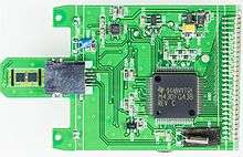
eZ430-F2013
TI has tackled the low-budget problem by offering a very small experimenter board, the eZ430-F2013, on a USB stick. This makes it easy for designers to choose the MSP430 chip for inexpensive development platforms that can be used with a computer. The eZ430-F2013 contains an MSP430F2013 microcontroller on a detachable prototyping board, and accompanying CD with development software. It is helpful for schools, hobbyists and garage inventors. It is also welcomed by engineers in large companies prototyping projects with capital budget problems.
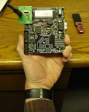
MSP430 LaunchPad
Texas Instruments released the MSP430 LaunchPad in July 2010. The MSP430 LaunchPad has an onboard flash emulator, USB, 2 programmable LEDs, and 1 programmable push button.[8] As an addition to experimentation with the LaunchPad a shield board is available.
TI has since provided several new LaunchPads based on the MSP430 platform:
- MSP-EXP430F5529LP features the MSP430F5529 USB device-capable MCU with 128KB flash and 8KB SRAM
- MSP-EXP430FR5969 features the MSP430FR5969 FRAM MCU with 64KB FRAM and 2KB SRAM
- MSP-EXP430FR4133 features the MSP430FR4133 FRAM MCU with 16KB FRAM, 2KB SRAM and on-board LCD
- MSP-EXP430FR6989 features the MSP430FR6989 FRAM MCU with 128KB FRAM, 2KB SRAM, on-board LCD and Extended Scan Interface peripheral
- MSP-EXP430FR2311 features the MSP430FR2311 FRAM MCU with 4KB FRAM, 1KB SRAM, OpAmp and Transimpedance Amplifier peripheral
- MSP-EXP430FR2433 features the MSP430FR2433 FRAM MCU with 15.5KB FRAM, 4KB SRAM
- MSP-EXP430FR2355 features the MSP430FR2355 FRAM MCU with 32KB FRAM, 4KB SRAM, 12-bit ADC, 12-bit DAC, OpAmp/PGA, ICC for nested interrupts
- MSP-EXP430FR5994 features the MSP430FR5994 FRAM MCU with 256KB FRAM, 8KB SRAM, 12-bit ADC and LEA DSP peripheral
All three of these LaunchPads include an eZ-FET JTAG debugger with backchannel UART capable of 1Mbit/s speeds. The FRAM LaunchPads (e.g. MSP-EXP430FR5969, MSP-EXP430FR4133) include EnergyTrace, a feature supported by TI's Code Composer Studio IDE for monitoring and analyzing power consumption.
Debugging interface
In common with other microcontroller vendors, TI has developed a two-wire debugging interface found on some of their MSP430 parts that can replace the larger JTAG interface. The eZ430 Development Tool contains a full USB-connected flash emulation tool ("FET") for this new two-wire protocol, named "Spy-Bi-Wire" by TI. Spy-Bi-Wire was initially introduced on only the smallest devices in the 'F2xx family with limited number of I/O pins, such as the MSP430F20xx, MSP430F21x2, and MSP430F22x2. The support for Spy-Bi-Wire has been expanded with the introduction of the latest '5xx family, where all devices have support Spy-Bi-Wire interface in addition to JTAG.
The advantage of the Spy-Bi-Wire protocol is that it uses only two communication lines, one of which is the dedicated _RESET line. The JTAG interface on the lower pin count MSP430 parts is multiplexed with general purpose I/O lines. This makes it relatively difficult to debug circuits built around the small, low-I/O-budget chips, since the full 4-pin JTAG hardware will conflict with anything else connected to those I/O lines. This problem is alleviated with the Spy-Bi-Wire-capable chips, which are still compatible with the normal JTAG interface for backwards compatibility with the old development tools.
JTAG debugging and flash programming tools based on OpenOCD and widely used in the ARM community are not available for the MSP430. Programming tools specially designed for the MSP430 are marginally less expensive than JTAG interfaces that use OpenOCD. However, should a project discover midstream that more MIPS, more memory, and more I/O peripherals are needed, those tools will not transfer to a processor from another vendor.
MSP430 CPU
The MSP430 CPU uses a von Neumann architecture, with a single address space for instructions and data. Memory is byte-addressed, and pairs of bytes are combined little-endian to make 16-bit words.
The processor contains 16 16-bit registers,[9] of which four are dedicated to special purposes: R0 is the program counter, R1 is the stack pointer, R2 is the status register, and R3 is a "constant generator" which reads as zero and ignores writes. Additional address mode encodings using R3 and R2 allow a total of six commonly used constant values (0, 1, 2, 4, 8 and −1) without requiring an immediate operand word. R4 through R15 are available for general use.
The instruction set is very simple; there are 27 instructions in three families. Most instructions are available in .B (8-bit byte) and .W (16-bit word) suffixed versions, depending on the value of a B/W bit: the bit is set to 1 for 8-bit and 0 for 16-bit. A missing suffix is equivalent to .W. Byte operations to memory affect only the addressed byte, while byte operations to registers clear the most significant byte.
| 15 | 14 | 13 | 12 | 11 | 10 | 9 | 8 | 7 | 6 | 5 | 4 | 3 | 2 | 1 | 0 | Instruction |
|---|---|---|---|---|---|---|---|---|---|---|---|---|---|---|---|---|
| 0 | 0 | 0 | 1 | 0 | 0 | opcode | B/W | As | register | Single-operand arithmetic | ||||||
| 0 | 0 | 0 | 1 | 0 | 0 | 0 | 0 | 0 | B/W | As | register | RRC Rotate right (1 bit) through carry | ||||
| 0 | 0 | 0 | 1 | 0 | 0 | 0 | 0 | 1 | 0 | As | register | SWPB Swap bytes | ||||
| 0 | 0 | 0 | 1 | 0 | 0 | 0 | 1 | 0 | B/W | As | register | RRA Rotate right (1 bit) arithmetic | ||||
| 0 | 0 | 0 | 1 | 0 | 0 | 0 | 1 | 1 | 0 | As | register | SXT Sign extend byte to word | ||||
| 0 | 0 | 0 | 1 | 0 | 0 | 1 | 0 | 0 | B/W | As | register | PUSH Push value onto stack | ||||
| 0 | 0 | 0 | 1 | 0 | 0 | 1 | 0 | 1 | 0 | As | register | CALL Subroutine call; push PC and move source to PC | ||||
| 0 | 0 | 0 | 1 | 0 | 0 | 1 | 1 | 0 | 0 | 0 | 0 | 0 | 0 | 0 | 0 | RETI Return from interrupt; pop SR then pop PC |
| 0 | 0 | 1 | condition | 10-bit signed offset | Conditional jump; PC = PC + 2×offset | |||||||||||
| 0 | 0 | 1 | 0 | 0 | 0 | 10-bit signed offset | JNE/JNZ Jump if not equal/zero | |||||||||
| 0 | 0 | 1 | 0 | 0 | 1 | 10-bit signed offset | JEQ/JZ Jump if equal/zero | |||||||||
| 0 | 0 | 1 | 0 | 1 | 0 | 10-bit signed offset | JNC/JLO Jump if no carry/lower | |||||||||
| 0 | 0 | 1 | 0 | 1 | 1 | 10-bit signed offset | JC/JHS Jump if carry/higher or same | |||||||||
| 0 | 0 | 1 | 1 | 0 | 0 | 10-bit signed offset | JN Jump if negative | |||||||||
| 0 | 0 | 1 | 1 | 0 | 1 | 10-bit signed offset | JGE Jump if greater or equal | |||||||||
| 0 | 0 | 1 | 1 | 1 | 0 | 10-bit signed offset | JL Jump if less | |||||||||
| 0 | 0 | 1 | 1 | 1 | 1 | 10-bit signed offset | JMP Jump (unconditionally) | |||||||||
| opcode | source | Ad | B/W | As | destination | Two-operand arithmetic | ||||||||||
| 0 | 1 | 0 | 0 | source | Ad | B/W | As | destination | MOV Move source to destination | |||||||
| 0 | 1 | 0 | 1 | source | Ad | B/W | As | destination | ADD Add source to destination | |||||||
| 0 | 1 | 1 | 0 | source | Ad | B/W | As | destination | ADDC Add source and carry to destination | |||||||
| 0 | 1 | 1 | 1 | source | Ad | B/W | As | destination | SUBC Subtract source from destination (with carry) | |||||||
| 1 | 0 | 0 | 0 | source | Ad | B/W | As | destination | SUB Subtract source from destination | |||||||
| 1 | 0 | 0 | 1 | source | Ad | B/W | As | destination | CMP Compare (pretend to subtract) source from destination | |||||||
| 1 | 0 | 1 | 0 | source | Ad | B/W | As | destination | DADD Decimal add source to destination (with carry) | |||||||
| 1 | 0 | 1 | 1 | source | Ad | B/W | As | destination | BIT Test bits of source AND destination | |||||||
| 1 | 1 | 0 | 0 | source | Ad | B/W | As | destination | BIC Bit clear (dest &= ~src) | |||||||
| 1 | 1 | 0 | 1 | source | Ad | B/W | As | destination | BIS Bit set (logical OR) | |||||||
| 1 | 1 | 1 | 0 | source | Ad | B/W | As | destination | XOR Exclusive or source with destination | |||||||
| 1 | 1 | 1 | 1 | source | Ad | B/W | As | destination | AND Logical AND source with destination (dest &= src) | |||||||
Instructions are 16 bits, followed by up to two 16-bit extension words. Addressing modes are specified by the 2-bit As field and the 1-bit Ad field. Some special versions can be constructed using R0, and modes other than register direct using R2 (the status register) and R3 (the constant generator) are interpreted specially. Ad can use only a subset of the addressing modes for As.
Indexed addressing modes add a 16-bit extension word to the instruction. If both source and destination are indexed, the source extension word comes first. x refers to the next extension word in the instruction stream in the table below.
| As | Ad | Register | Syntax | Description |
|---|---|---|---|---|
| 00 | 0 | n | Rn | Register direct. The operand is the contents of Rn. |
| 01 | 1 | n | x(Rn) | Indexed. The operand is in memory at address Rn+x. |
| 10 | — | n | @Rn | Register indirect. The operand is in memory at the address held in Rn. |
| 11 | — | n | @Rn+ | Indirect autoincrement. As above, then the register is incremented by 1 or 2. |
| Addressing modes using R0 (PC) | ||||
| 01 | 1 | 0 (PC) | ADDR | Symbolic. Equivalent to x(PC). The operand is in memory at address PC+x. |
| 11 | — | 0 (PC) | #x | Immediate. Equivalent to @PC+. The operand is the next word in the instruction stream. |
| Addressing modes using R2 (SR) and R3 (CG), special-case decoding | ||||
| 01 | 1 | 2 (SR) | &ADDR | Absolute. The operand is in memory at address x. |
| 10 | — | 2 (SR) | #4 | Constant. The operand is the constant 4. |
| 11 | — | 2 (SR) | #8 | Constant. The operand is the constant 8. |
| 00 | — | 3 (CG) | #0 | Constant. The operand is the constant 0. |
| 01 | — | 3 (CG) | #1 | Constant. The operand is the constant 1. There is no index word. |
| 10 | — | 3 (CG) | #2 | Constant. The operand is the constant 2. |
| 11 | — | 3 (CG) | #−1 | Constant. The operand is the constant −1. |
Instructions generally take 1 cycle per word fetched or stored, so instruction times range from 1 cycle for a simple register-register instruction to 6 cycles for an instruction with both source and destination indexed.
The MSP430X extension with 20-bit addressing adds additional instructions that can require up to 10 clock cycles. Setting or clearing a peripheral bit takes two clocks. A jump, taken or not takes two clocks. With the 2xx series 2 MCLKs is 125 ns at 16 MHz.
Moves to the program counter are allowed and perform jumps. Return from subroutine, for example, is implemented as MOV @SP+,PC.
When R0 (PC) or R1 (SP) are used with the autoincrement addressing mode, they are always incremented by two. Other registers (R4 through R15) are incremented by the operand size, either 1 or 2 bytes.
The status register contains 4 arithmetic status bits, a global interrupt enable, and 4 bits that disable various clocks to enter low-power mode. When handling an interrupt, the processor saves the status register on the stack and clears the low-power bits. If the interrupt handler does not modify the saved status register, returning from the interrupt will then resume the original low-power mode.
Pseudo-operations
A number of additional instructions are implemented as aliases for forms of the above. For example, there is no specific "return from subroutine" instruction, but it is implemented as "MOV @SP+,PC". Emulated instructions are:
| Emulated | Actual | Description |
|---|---|---|
| ADC.x dst | ADDC.x #0,dst | Add carry to destination |
| BR dst | MOV dst,PC | Branch to destination |
| CLR.x dst | MOV.x #0,dst | Clear destination |
| CLRC | BIC #1,SR | Clear carry bit |
| CLRN | BIC #4,SR | Clear negative bit |
| CLRZ | BIC #2,SR | Clear zero bit |
| DADC.x dst | DADD.x #0,dst | Decimal add carry to destination |
| DEC.x dst | SUB.x #1,dst | Decrement |
| DECD.x dst | SUB.x #2,dst | Double decrement |
| DINT | BIC #8,SR | Disable interrupts |
| EINT | BIS #8,SR | Enable interrupts |
| INC.x dst | ADD.x #1,dst | Increment |
| INCD.x dst | ADD.x #2,dst | Double increment |
| INV.x dst | XOR.x #−1,dst | Invert |
| NOP | MOV #0,R3 | No operation |
| POP dst | MOV @SP+,dst | Pop from stack |
| RET | MOV @SP+,PC | Return from subroutine |
| RLA.x dst | ADD.x dst,dst | Rotate left arithmetic (shift left 1 bit) |
| RLC.x dst | ADDC.x dst,dst | Rotate left through carry |
| SBC.x dst | SUBC.x #0,dst | Subtract borrow (1−carry) from destination |
| SETC | BIS #1,SR | Set carry bit |
| SETN | BIS #4,SR | Set negative bit |
| SETZ | BIS #2,SR | Set zero bit |
| TST.x dst | CMP.x #0,dst | Test destination |
Note that the immediate constants −1 (0xffff), 0, 1, 2, 4 and 8 can be specified in a single-word instruction without needing a separate immediate operand.
MSP430X 20-bit extension
The basic MSP430 cannot support more memory (ROM + RAM + peripherals) than its 64K address space. In order to support this, an extended form of the MSP430 uses 20-bit registers and a 20-bit address space, allowing up to 1 MB of memory. This uses the same instruction set as the basic form, but with two extensions:
- A limited number of 20-bit instructions for common operations, and
- A general prefix-word mechanism that can extend any instruction to 20 bits.
The extended instructions include some additional capabilities, notably multi-bit shifts and multi-register load/store operations.
20-bit operations use the length suffix "A" (for address) instead of .B or .W. .W is still the default. In general, shorter operations clear the high-order bits of the destination register.
The new instructions are as follows:
| 15 | 14 | 13 | 12 | 11 | 10 | 9 | 8 | 7 | 6 | 5 | 4 | 3 | 2 | 1 | 0 | Second word | Instruction |
|---|---|---|---|---|---|---|---|---|---|---|---|---|---|---|---|---|---|
| 0 | 0 | 0 | 0 | source | 0 | 0 | opcode | destination | Extended memory-register moves | ||||||||
| 0 | 0 | 0 | 0 | src | 0 | 0 | 0 | 0 | dst | — | MOVA @Rsrc,Rdst | ||||||
| 0 | 0 | 0 | 0 | src | 0 | 0 | 0 | 1 | dst | — | MOVA @Rsrc+,Rdst | ||||||
| 0 | 0 | 0 | 0 | addr[19:16] | 0 | 0 | 1 | 0 | dst | addr[15:0] | MOVA &abs20,Rdst | ||||||
| 0 | 0 | 0 | 0 | src | 0 | 0 | 1 | 1 | dst | x[15:0] | MOVA x(Rsrc),Rdst | ||||||
| 0 | 0 | 0 | 0 | n−1 | op. | 0 | 1 | 0 | W/A | destination | Bit shifts (1–4 bit positions) | ||||||
| 0 | 0 | 0 | 0 | n−1 | 0 | 0 | 0 | 1 | 0 | W/A | dst | — | RRCM.x #n,Rdst (Rotate right through carry.) | ||||
| 0 | 0 | 0 | 0 | n−1 | 0 | 1 | 0 | 1 | 0 | W/A | dst | — | RRAM.x #n,Rdst (Rotate right arithmetic, a.k.a. shift right signed.) | ||||
| 0 | 0 | 0 | 0 | n−1 | 1 | 0 | 0 | 1 | 0 | W/A | dst | — | RLAM.x #n,Rdst (Rotate left arithmetic, a.k.a. shift left.) | ||||
| 0 | 0 | 0 | 0 | n−1 | 1 | 1 | 0 | 1 | 0 | W/A | dst | — | RRUM.x #n,Rdst (Rotate right unsigned, a.k.a. shift right logical.) | ||||
| 0 | 0 | 0 | 0 | source | 0 | 1 | 1 | op. | destination | Extended register-memory moves | |||||||
| 0 | 0 | 0 | 0 | src | 0 | 1 | 1 | 0 | addr[19:16] | addr[15:0] | MOVA Rsrc,&abs20 | ||||||
| 0 | 0 | 0 | 0 | src | 0 | 1 | 1 | 1 | dst | x[15:0] | MOVA Rsrc,x(Rdst) | ||||||
| 0 | 0 | 0 | 0 | source | 1 | opcode | destination | Extended ALU operations | |||||||||
| 0 | 0 | 0 | 0 | imm[19:16] | 1 | 0 | 0 | 0 | dst | imm[15:0] | MOVA #imm20,Rdst | ||||||
| 0 | 0 | 0 | 0 | imm[19:16] | 1 | 0 | 0 | 1 | dst | imm[15:0] | CMPA #imm20,Rdst | ||||||
| 0 | 0 | 0 | 0 | imm[19:16] | 1 | 0 | 1 | 0 | dst | imm[15:0] | ADDA #imm20,Rdst | ||||||
| 0 | 0 | 0 | 0 | imm[19:16] | 1 | 0 | 1 | 1 | dst | imm[15:0] | SUBA #imm20,Rdst | ||||||
| 0 | 0 | 0 | 0 | src | 1 | 1 | 0 | 0 | dst | — | MOVA Rsrc,Rdst | ||||||
| 0 | 0 | 0 | 0 | src | 1 | 1 | 0 | 1 | dst | — | CMPA Rsrc,Rdst | ||||||
| 0 | 0 | 0 | 0 | src | 1 | 1 | 1 | 0 | dst | — | ADDA Rsrc,Rdst | ||||||
| 0 | 0 | 0 | 0 | src | 1 | 1 | 1 | 1 | dst | — | SUBA Rsrc,Rdst | ||||||
| 0 | 0 | 0 | 1 | 0 | 0 | 1 | 1 | op. | mode | varies | CALLA | ||||||
| 0 | 0 | 0 | 1 | 0 | 0 | 1 | 1 | 0 | 0 | 0 | 0 | 0 | 0 | 0 | 0 | — | RETI (Same as MSP430) |
| 0 | 0 | 0 | 1 | 0 | 0 | 1 | 1 | 0 | 1 | As | register | CALLA source | |||||
| 0 | 0 | 0 | 1 | 0 | 0 | 1 | 1 | 1 | 0 | 0 | 0 | abs[19:16] | abs[15:0] | CALLA &abs20 | |||
| 0 | 0 | 0 | 1 | 0 | 0 | 1 | 1 | 1 | 0 | 0 | 1 | x[19:16] | x[15:0] | CALLA x(PC) | |||
| 0 | 0 | 0 | 1 | 0 | 0 | 1 | 1 | 1 | 0 | 1 | 0 | — | — | (reserved) | |||
| 0 | 0 | 0 | 1 | 0 | 0 | 1 | 1 | 1 | 0 | 1 | 1 | imm[19:16] | imm[15:0] | CALLA #imm20 | |||
| 0 | 0 | 0 | 1 | 0 | 0 | 1 | 1 | 1 | 1 | — | — | (reserved) | |||||
| 0 | 0 | 0 | 1 | 0 | 1 | dir | W/A | n−1 | register | Push/pop n registers ending with specified | |||||||
| 0 | 0 | 0 | 1 | 0 | 1 | 0 | W/A | n−1 | src | — | PUSHM.x #n,Rsrc Push Rsrc, R(src−1), ... R(src−n+1) | ||||||
| 0 | 0 | 0 | 1 | 0 | 1 | 1 | W/A | n−1 | dst−n+1 | — | POPM.x #n,Rdst Pop R(dst−n+1), R(dst−n+2), ... Rdst | ||||||
All other instructions can have a prefix word added which extends them to 20 bits. The prefix word contains an additional operand size bit, which is combined with the existing B/W bit to specify the operand size. There is one unused size combination; there are indications that this might be used in future for a 32-bit operand size.[10]
The prefix word comes in two formats, and the choice between them depends on the instruction which follows. If the instruction has any non-register operands, then the simple form is used, which provides 2 4-bit fields to extend any offset or immediate constant in the instruction stream to 20 bits.
If the instruction is register-to-register, a different extension word is used. This includes a "ZC" flag which suppresses carry-in (useful for instructions like DADD which always use the carry bit), and a repeat count. A 4-bit field in the extension word encodes either a repeat count (0–15 repetitions in addition to the initial execution), or a register number which contains a 4-bit repeat count.
| 15 | 14 | 13 | 12 | 11 | 10 | 9 | 8 | 7 | 6 | 5 | 4 | 3 | 2 | 1 | 0 | Instruction |
|---|---|---|---|---|---|---|---|---|---|---|---|---|---|---|---|---|
| 0 | 0 | 0 | 1 | 1 | — | A/L | 0 | 0 | — | Extension word | ||||||
| 0 | 0 | 0 | 1 | 1 | src[19:16] | A/L | 0 | 0 | dst[19:16] | Memory operand extension | ||||||
| 0 | 0 | 0 | 1 | 1 | 0 | 0 | ZC | 0 | A/L | 0 | 0 | n−1 | Register operand extension (immediate repeat count) | |||
| 0 | 0 | 0 | 1 | 1 | 0 | 0 | ZC | 1 | A/L | 0 | 0 | Rn | Register operand extension (register repeat count) | |||
MSP430 address space
The general layout of the MSP430 address space is:
- 0x0000–0x0007
- Processor special function registers (interrupt control registers)
- 0x0008–0x00FF
- 8-bit peripherals. These must be accessed using 8-bit loads and stores.
- 0x0100–0x01FF
- 16-bit peripherals. These must be accessed using 16-bit loads and stores.
- 0x0200–0x09FF
- Up to 2048 bytes of RAM.
- 0x0C00–0x0FFF
- 1024 bytes of bootstrap loader ROM (flash parts only).
- 0x1000–0x10FF
- 256 bytes of data flash ROM (flash parts only).
- 0x1800-0x19FF
- 512 bytes of data FRAM (most FRAM MCUs, user-writable containing no calibration data)
- 0x1100–0x38FF
- Extended RAM on models with more than 2048 bytes of RAM. (0x1100–0x18FF is a copy of 0x0200–0x09FF)
- 0x1100–0xFFFF
- Up to 60 kilobytes of program ROM. Smaller ROMs start at higher addresses. The last 16 or 32 bytes are interrupt vectors.
A few models include more than 2048 bytes of RAM; in that case RAM begins at 0x1100. The first 2048 bytes (0x1100–0x18FF) is mirrored at 0x0200–0x09FF for compatibility. Also, some recent models bend the 8-bit and 16-bit peripheral rules, allowing 16-bit access to peripherals in the 8-bit peripheral address range.
There is a new extended version of the architecture (called MSP430X) which allows a 20-bit address space. It allows additional program ROM beginning at 0x10000.
The '5xx series has a greatly redesigned address space, with the first 4K devoted to peripherals, and up to 16K of RAM.
References
- MSP430 will run on grapes – video on YouTube
- D. Peters, D. Raskovic, and D. Thorsen, "An Energy Efficient Parallel Embedded System for Small Satellite Applications", ISAST Transactions on Computers and Intelligent Systems, vol. 1(2), 2009
- Lowest Power MSP430 Microcontrollers from Texas Instruments
- http://www.ti.com/lit/slau445
- , Energia website
- MSP430 article published in IEEE magazine.
- Visual Solutions
- MSP430 LaunchPad (MSP-EXP430G2), Texas Instruments Embedded Processors Wiki
- "MSP430 Ultra-Low-Power Microcontroller" (PDF). Texas Instruments. Retrieved 9 July 2008.
- The size bit itself is named "A/L", where "L" (long) is used by other processors to indicate 32-bit operands. Also the description of the SXTX instruction (MSP430F5xx Family User's Guide alau208f page 237) describes the effect of the instruction in register bits 20–31.
External links
Community and information sites
- TI MSP430 Homepage
- TI E2E MSP430 Community forum
- MSP430 Community sponsored by Texas Instruments
- MSP430 Yahoo!group
- MSP430.info
- MSP430 English-Japanese forum
- 43oh.com – MSP430 News, Projects and Forums
- TinyOS-MSP430 TinyOS port
- MSP430 Egel project pages – About 50 examples with sources, schematics, well documented.
Visual programming C code generators
Compilers, assemblers and IDEs
Free Compiler and IDEs
- Arduino IDE Arduino IDE
- Code Composer Studio Eclipse based IDE
- Code Composer Studio Cloud
- IAR Embedded Workbench Kickstart IDE (size limited to 4/8/16 KB – depends on device used)
- GCC toolchain for the MSP430 Microcontrollers
- MSP430 Development System
- naken_asm Open-Source MSP430 assembler, disassembler, simulator.
- Pre-built MSP430 GCC 4.x binaries for Windows
- MSP430 16-bit noForth compiler With assembler, disassembler and sources.
- FastForth with 5 MBds terminal, assembler, SD_Card driver...
Most popular unrestricted IDEs and compilers
- IAR Embedded Workbench for TI MSP430
- Rowley CrossWorks for MSP430 (only a 30-day evaluation period)
- GCC toolchain for the MSP430 Microcontrollers (Free C-compiler)
- MSP430 Development System
- A plugin for Visual Studio that supports MSP430 via MSP430-GCC (30-day evaluation)
Miscellaneous IDEs
- AQ430 Development Tools for MSP430 Microcontrollers
- ImageCraft C Tools
- ForthInc Forth-Compiler
- MPE Forth IDE & Cross-Compiler for MSP430 currently in Beta
- HI-TECH C for MSP430 (Dropped MSP430 Support in 2009)
List of debugging tools (not complete)
| Name | Manufacturer | Interface | Protocol(s) | Status |
|---|---|---|---|---|
| MSP-FET430PIF | TI | Parallel-Port | JTAG | |
| MSP-FET430UIF | TI | USB-Interface | JTAG, Spy-Bi-Wire | |
| MSP-FET | TI | USB-Interface | JTAG, Spy-Bi-Wire | |
| MSP-430 LaunchPad | TI | USB-Interface | Spy-Bi-Wire | |
| MSP-430 LaunchPad eZ-FET | TI | USB-Interface | Spy-Bi-Wire | |
| eZ430-F2013 | TI | USB-Interface | Spy-Bi-Wire | |
| eZ430-RF2500 | TI | USB-Interface | Spy-Bi-Wire | |
| FETP | SoftBaugh | Parallel-Port | JTAG | |
| USBP | SoftBaugh | USB-Interface | JTAG, Spy-Bi-Wire | discontinued |
| MSP430-JTAG | Olimex | Parallel-Port | JTAG | |
| MSP430-JTAG-ISO | Olimex | USB-Interface | JTAG, Spy-Bi-Wire | obsolete |
| MSP430-JTAG-ISO-MK2 | Olimex | USB-Interface | JTAG, Spy-Bi-Wire | |
| MSP430-JTAG-Tiny | Olimex | USB-Interface | JTAG, Spy-Bi-Wire | not found |
| MSP430-JTAG-TINY-V2 | Olimex | USB-Interface | JTAG?, Spy-Bi-Wire | |
| MSP430-JTAG-RF | Olimex | USB-Interface | JTAG, Spy-Bi-Wire | |
| FlashPro-CC | Elprotronic | USB-Interface | JTAG, Spy-Bi-Wire, BSL | |
| VisSim/ECD | Visual Solutions | USB-Interface | JTAG, Spy-Bi-Wire | |
| LA-3713 | Lauterbach | USB-Interface / Ethernet | JTAG, Spy-bi-Wire | |
Other tools
- WSim – a software-driven emulator for full platform estimations and debug
- MSPSim – a Java based MSP430 emulator/simulator
- MSP430Static – a reverse engineering tool in Perl
- GoodFET – an open MSP430 JTAG debugger in C and Python
- mspdebug – an opensource MSP430 JTAG debugger
- Trace32 MSP430 SIM – Download area with MSP430 Instruction Set Simulator free for evaluation
- ERIKA Enterprise – a free of charge, open source RTOS implementation of the ISO 17356 API (derived from the OSEK/VDX API)
- Energia is based on Wiring and Arduino and uses the Processing IDE. The hardware platform is based upon TI MSP430 LaunchPad