Slot-waveguide
A slot-waveguide is an optical waveguide that guides strongly confined light in a subwavelength-scale low refractive index region by total internal reflection.
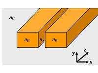
A slot-waveguide consists of two strips or slabs of high-refractive-index (nH) materials separated by a subwavelength-scale low-refractive-index (nS) slot region and surrounded by low-refractive-index (nC) cladding materials.

Principle of operation
The principle of operation of a slot-waveguide is based on the discontinuity of the electric field (E-field) at high-refractive-index-contrast interfaces. Maxwell’s equations state that, to satisfy the continuity of the normal component of the electric displacement field D at an interface, the corresponding E-field must undergo a discontinuity with higher amplitude in the low-refractive-index side. That is, at an interface between two regions of dielectric constants εS and εH, respectively:
- DSN=DHN
- εSESN=εHEHN
- nS2ESN=nH2EHN
where the superscript N indicates the normal components of D and E vector fields. Thus, if nS<<nH, then ESN>>EHN.
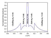
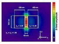
Given that the slot critical dimension (distance between the high-index slabs or strips) is comparable to the exponential decay length of the fundamental eigenmode of the guided-wave structure, the resulting E-field normal to the high-index-contrast interfaces is enhanced in the slot and remains high across it. The power density in the slot is much higher than that in the high-index regions. Since wave propagation is due to total internal reflection, there is no interference effect involved and the slot-structure exhibits very low wavelength sensitivity.[1]
Invention
The slot-waveguide was born in 2003 as an unexpected outcome of theoretical studies on metal-oxide-semiconductor (MOS) electro-optic modulation in high-confinement silicon photonic waveguides by Vilson Rosa de Almeida and Carlos Angulo Barrios, then a Ph.D. student and a Postdoctoral Associate, respectively, at Cornell University. Theoretical analysis [1] and experimental demonstration [2] of the first slot-waveguide implemented in the Si/SiO2 material system at 1.55 μm operation wavelength were reported by Cornell researchers in 2004.
Since these pioneering works, several guided-wave configurations based on the slot-waveguide concept have been proposed and demonstrated. Relevant examples are the following:
In 2005, researchers at the Massachusetts Institute of Technology proposed to use multiple slot regions in the same guided-wave structure (multi-slot waveguide) in order to increase the optical field in the low-refractive-index regions.[3] The experimental demonstration of such multiple slot waveguide in a horizontal configuration was first published in 2007.[4]
In 2006, the slot-waveguide approach was extended to the terahertz frequency band by researchers at RWTH Aachen University.[5] Researchers at the California Institute of Technology also demonstrated that a slot waveguide, in combination with nonlinear electrooptic polymers, could be used to build ring modulators with exceptionally high tunability.[6] Later this same principle enabled Baehr-Jones et al. to demonstrate a mach-zehnder modulator with an exceptionally low drive voltage of 0.25 V[7][8]
In 2007, a non-planar implementation of the slot-waveguide principle of operation was demonstrated by researchers at the University of Bath. They showed concentration of optical energy within a subwavelength-scale air hole running down the length of a photonic-crystal fiber.[9]
Recently, in 2016, it is shown [10] that slots in a pair of waveguides if off-shifted away from each other can enhance the coupling coefficient even more than 100% if optimized properly, and thus the effective power coupling length between the waveguides can significantly be reduced. Hybrid slot (having vertical slot in one waveguide and horizontal slot in the other) assisted polarization beam splitter is also numerically demonstrated. Though, the losses are high for such slot structures, this scheme exploiting the asymmetric slots may have potential to design very compact optical directional couplers and polarization beam splitters for on-chip integrated optical devices.
Fabrication
Planar slot-waveguides have been fabricated in different material systems such as Si/SiO2[2][11][12] and Si3N4/SiO2.[13] Both vertical (slot plane is normal to the substrate plane) and horizontal (slot plane is parallel to the substrate plane) configurations have been implemented by using conventional micro- and nano-fabrication techniques. These processing tools include electron beam lithography, photolithography, chemical vapour deposition [usually low-pressure chemical vapour deposition (LPCVD) or plasma enhanced chemical vapour deposition (PECVD)], thermal oxidation, reactive-ion etching and focused ion beam.
In vertical slot-waveguides, the slot and strips widths are defined by electron- or photo-lithography and dry etching techniques whereas in horizontal slot-waveguides the slot and strips thicknesses are defined by a thin-film deposition technique or thermal oxidation. Thin film deposition or oxidation provides better control of the layers dimensions and smoother interfaces between the high-index-contrast materials than lithography and dry etching techniques. This makes horizontal slot-waveguides less sensitive to scattering optical losses due to interface roughness than vertical configurations.
Fabrication of a non-planar (fiber-based) slot-waveguide configuration has also been demonstrated by means of conventional microstructured optical fiber technology.[9]
Applications
A slot-waveguide produces high E-field amplitude, optical power, and optical intensity in low-index materials at levels that cannot be achieved with conventional waveguides. This property allows highly efficient interaction between fields and active materials, which may lead to all-optical switching,[14] optical amplification [15][16] and optical detection [6] on integrated photonics. Strong E-field confinement can be localized in a nanometer-scale low-index region. As firstly pointed out in,[1] the slot waveguide can be used to greatly increase the sensitivity of compact optical sensing devices [17][18][19][20][21][22] or to enhance the efficiency of near-field optics probes. At Terahertz frequencies, slot waveguide based splitter has been designed which allows for low loss propagation of Terahertz waves. The device acts as a splitter through which maximum throughput can be achieved by adjusting the arm length ratio of the input to the output side.[23]
References
- 1 2 3 V.R. Almeida, Q. Xu, C.A. Barrios, and M. Lipson, “Guiding and confining Light in void nanostructure,” Optics Letters, vol. 29, no. 11, pp. 1209-1211, 2004.
- 1 2 Q. Xu, V.R. Almeida, R.R. Panepucci, and M. Lipson, “Experimental demonstration of guiding and confining light in nanometer-size low-refractive-index material,” Optics Letters, vol. 29, no. 14, pp. 1626-1628, 2004.
- ↑ N.-N. Feng, J. Michel, and L.C. Kimerling, “Optical field concentration in low-index waveguides,” IEEE J. Quantum Electron. 42 (9), p. 885, 2006.
- ↑ R. Sun, P. Dong, N.-N. Feng, C.-Y. Hong, J. Michel, M. Lipson, and L.C. Kimerling, "Horizontal single and multiple slot waveguides: optical transmission at λ = 1550 nm," Optics Express 15, 17967, 2007
- ↑ M. Nagel, A. Marchewka, and H. Kurz, “Low-index discontinuity terahertz waveguides,” Optics Express, 14(21), p. 9944, 2006.
- 1 2 T. Baehr-Jones, M. Hochberg, G. Wang, R. Lawson, Y. Liao, P. A. Sullivan, L. Dalton, A. K.-Y. Jen, and A. Scherer, “Optical modulation and detection in slotted silicon waveguides,” Opt. Express 13, 5216-5226 (2005).
- ↑ T. Baehr-Jones, B. Penkov, J. Huang, P. Sullivan, J. Davies, J. Takayesu, J. Luo, T.-D. Kim, L. Dalton, A. Jen, M. Hochberg, and A. Scherer, "Nonlinear polymer-clad silicon slot waveguide modulator with a half wave voltage of 0.25 V," Applied Physics Letters 92, 163303 (2008).
- ↑ J. Witzens, T. Baehr-Jones, M. Hochberg, "Design of transmission line driven slot waveguide Mach-Zehnder interferometers and applications to analog optical links", Opt. Express 18, 16902-16928 (2010).
- 1 2 G.S. Wiederhecker, C.M.B. Cordeiro, F. County, F. Benabid, S.A. Maier, J.C. Knight, C.H.B. Cruz and H.L. Fragnito, “Field enhancement within an optical fibre with a subwavelength air core,” Nature Photonics, 1, 115-118 (2007).
- ↑ Raktim Haldar, V. Mishra, A. Dutt, S. K. Varshney, “On-chip broadband ultra-compact optical couplers and polarization splitters based on off-centered and non-symmetric slotted Si-wire waveguides,” in Journal of Optics, IOP Science, vol. 18, no. 10, 105801, September, 2016
- ↑ T. Baehr-Jones, M. Hochberg, C. Walker, A Scherer, “High-Q optical resonators in silicon-on-insulator based slot waveguides,” Appl. Phys. Lett. 86, 081101 (2005).
- ↑ Schrauwen J., Van Lysebettens J., Vanhoutte M., Van Thourhout D. et al., "Iodine enhanced focused ion beam etching of silicon for photonic device modification and prototyping (2008)", International Workshop on FIB for Photonics, 1st, Proceedings (2008)
- ↑ C.A. Barrios, B. Sanchez, K.B. Gylfason, A. Griol, H. Sohlström, M. Holgado and R. Casquel “Demonstration of slot-waveguides structures on silicon nitride/silicon oxide platform,” Optics Express, 15(11), pp.6846-6856, 2007.
- ↑ C.A. Barrios, “High-performance all-optical silicon microswitch,” Electronics Letters, 40 (14), 862-863 (2004).
- ↑ C.A. Barrios and M. Lipson, “Electrically driven silicon resonant light emitting device based on slot-waveguide,” Optics. Express 13, 10092-10101, (2005).
- ↑ A. Armaroli, A. Morand, P. Benech, G. Bellanca, S. Trillo, "Comparative Analysis of a Planar Slotted Microdisk Resonator," Lightwave Technology, Journal of , vol.27, no.18, pp.4009,4016, Sept.15, 2009
- ↑ C.A. Barrios, “Ultrasensitive nanomechanical photonic sensor based on horizontal slot-waveguide resonator,” IEEE Photon. Technol. Lett. 18, 2419-2421 (2006).
- ↑ C.A. Barrios, K.B. Gylfason, B. Sanchez, A. Griol, H. Sohlström, M. Holgado and R. Casquel, “Slot-waveguide biochemical sensor,” Optics Letters, 32(21), pp. 3080-3082, 2007.
- ↑ Francesco Dell’Olio and Vittorio M. N. Passaro. “Optical sensing by optimized silicon slot waveguides," Optics Express, vol. 15, Issue 8, pp.4977-4993, 2007
- ↑ C.A. Barrios, M.J. Bañuls, V. Gonzalez-Pedro, K.B. Gylfason, B. Sánchez, A. Griol, A. Maquieira, H. Sohlström, M. Holgado, and R. Casquel. “Label-free optical sensing with slot-waveguides,” Optics Letters, 33(7), pp. 708-710, 2008.
- ↑ J.T. Robinson, L. Chen, and M. Lipson, “On-chip gas detection in silicon optical microcavities,” Optics Express, 16 (6), pp. 4296-4301, 2008.
- ↑ J. Witzens, M. Hochberg, "Optical detection of target molecule induced aggregation of nanoparticles by means of high-Q resonators," Opt. Express 19, 7034-7061 (2011).
- ↑ Shashank Pandey, Gagan Kumar, and Ajay Nahata, "Slot waveguide-based splitters for broadband terahertz radiation," Opt. Express 18, 23466-23471 (2010).