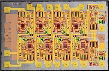
Planar process
The planar process is a manufacturing process used in the semiconductor industry to build individual components of a transistor, and in turn, connect those transistors together. It is the primary process by which modern integrated circuits are built. The process was developed[1][2] by Jean Hoerni, one of the "traitorous eight", while working at Fairchild Semiconductor, with a first patent issued 1959.
The key concept was to view a circuit in its two-dimensional projection (a plane), thus allowing the use of photographic processing concepts such as film negatives to mask the projection of light exposed chemicals. This allowed the use of a series of exposures on a substrate (Silicon) to create silicon oxide (insulators) or doped regions (conductors). Together with the use of metallization (to join together the integrated circuits), and the concept of p–n junction isolation (from Kurt Lehovec), the researchers at Fairchild were able to create circuits on a single silicon crystal slice (a wafer) from a monocrystalline silicon boule.
The process involves the basic procedures of silicon dioxide (SiO2) oxidation, SiO2 etching and heat diffusion. The final steps involves oxidizing the entire wafer with an SiO2 layer, etching contact vias to the transistors, and depositing a covering metal layer over the oxide, thus connecting the transistors without manually wiring them together.
Early versions of the planar process used a photolithography process using near-ultraviolet light from a mercury vapor lamp. As of 2011, small features are typically made with 193 nm "deep" UV lithography.[3] Some researchers use even higher-energy extreme ultraviolet lithography.
See also
References
- ↑ US 3025589 Hoerni, J. A.: "Method of Manufacturing Semiconductor Devices” filed May 1, 1959
- ↑ US 3064167 Hoerni, J. A.: "Semiconductor device" filed May 15, 1960
- ↑ Shannon Hill. "UV Lithography: Taking Extreme Measures". National Institute of Standards and Technology (NIST).
External links
- "The silicon engine: A timeline of semiconductors in computing". Timeline: Browse by decade. Computer history museum. 2012. Retrieved 2012-06-03. A compendium of articles and other information on the development of integrated circuits, including the development of oxide masking, photolithography, the advent of silicon, the integrated circuit and the planar process.
- The Planar Process
- "The history of the integrated circuit". Nobelprize.org. 2003. Retrieved 2012-06-03. An overview of the steps in fabrication of an integrated circuit from the Nobel Prize website. This is a section of the work Techville: The integrated circuit.