Nitrogen-vacancy center
The nitrogen-vacancy center (N-V center) is one of numerous point defects in diamond. Its most explored and useful property is photoluminescence, which can be easily detected from an individual N-V center, especially those in the negative charge state (N-V−). Electron spins at N-V centers, localized at atomic scales, can be manipulated at room temperature by applying a magnetic field, electric field, microwave radiation or light, or a combination, resulting in sharp resonances in the intensity and wavelength of the photoluminescence. These resonances can be explained in terms of electron spin related phenomena such as quantum entanglement, spin-orbit interaction and Rabi oscillations, and analysed using advanced quantum optics theory. An individual N-V center can be viewed as a basic unit of a quantum computer, and it has potential applications in novel, more efficient fields of electronics and computational science including quantum cryptography, spintronics, steadystomics and masers.
Structure
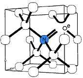
The nitrogen-vacancy center is a point defect in the diamond lattice. It consists of a nearest-neighbor pair of a nitrogen atom, which substitutes for a carbon atom, and a lattice vacancy.
Two charge states of this defect, neutral N-V0 and negative N-V−, are known from spectroscopic studies using optical absorption,[2][3] photoluminescence (PL),[4] electron paramagnetic resonance (EPR)[5][6][7] and optically detected magnetic resonance (ODMR),[8] which can be viewed as a hybrid of PL and EPR; most details of the structure originate from EPR. A nitrogen atom has five valence electrons. Three of them covalently bond to the carbon atoms and two remain non-bonded and are called a lone pair. The vacancy has three unpaired electrons. Two of them make a quasi covalent bond and one remains unpaired. The overall symmetry, however, is axial (trigonal C3V); one can visualize this by imagining the three unpaired vacancy electrons continuously exchanging their roles.
The N-V0 thus has one unpaired electron and is paramagnetic. However, despite extensive efforts, electron paramagnetic resonance signals from N-V0 avoided detection for decades until 2008. Optical excitation is required to bring the N-V0 defect into the EPR-detectable excited state; the signals from the ground state are presumably too broad for EPR detection.[9]
The N-V0 centers can be converted into N-V− by changing the Fermi level position. This can be achieved by applying external voltage to a p-n junction made from doped diamond, e.g., in a Schottky diode.[1]
In the negative charge state N-V−, an extra electron is located at the vacancy site forming a spin S=1 pair with one of the vacancy electrons. As in N-V0, the vacancy electrons are "exchanging roles" preserving the overall trigonal symmetry. This N-V− state is what is commonly, and somewhat incorrectly, called "the nitrogen-vacancy center". The neutral state has not yet been explored for spin manipulations.
The N-V centers are randomly oriented within a diamond crystal. Ion implantation techniques can enable their artificial creation in predetermined positions.[10]
Production
Nitrogen-vacancy centers are typically produced from single substitutional nitrogen centers (called C or P1 centers in diamond literature) by irradiation followed by annealing at temperatures above 700 °C.[2] A wide range of high-energy particles are suitable for such irradiation, including electrons, protons, neutrons, ions, and gamma photons. Irradiation produces lattice vacancies, which are a part of N-V centers. Those vacancies are immobile at room temperature, and annealing is required to move them. Single substitutional nitrogen produces strain in the diamond lattice;[11] it therefore efficiently captures moving vacancies,[12] producing the N-V centers.
During chemical vapor deposition of diamond, a small fraction of single substitutional nitrogen impurity (typically <0.5%) traps vacancies generated as a result of the plasma synthesis. Such nitrogen-vacancy centers are preferentially aligned to the growth direction.[13]
Diamond is notorious for having a relatively large lattice strain. Strain splits and shifts optical transitions from individual centers resulting in broad lines in the ensembles of centers.[2] Special care is taken to produce extremely sharp N-V lines (line width ~10 MHz)[14] required for most experiments: high-quality, pure natural or better synthetic diamonds (type IIa) are selected. Many of them already have sufficient concentrations of grown-in N-V centers and are suitable for applications. If not, they are irradiated by high-energy particles and annealed. Selection of a certain irradiation dose allows tuning the concentration of produced N-V centers such that individual N-V centers are separated by micrometre-large distances. Then, individual N-V centers can be studied with standard optical microscopes or, better, near-field scanning optical microscopes having sub-micrometre resolution.[8][15]
Basic optical properties
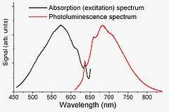
N-V− centers emit bright red light which can be conveniently excited by visible light sources, such as argon or krypton lasers, frequency doubled Nd:YAG lasers, dye lasers, or He-Ne lasers. Excitation can also be achieved at energies below that of zero phonon emission.[16] Laser illumination, however, also converts some N-V− into N-V0 centers.[4] Emission is very quick (relaxation time ~10 ns).[17][18] At room temperature, no sharp peaks are observed because of the thermal broadening. However, cooling the N-V− centers with liquid nitrogen or liquid helium dramatically narrows the lines down to a width of a few megahertz.
An important property of the luminescence from individual N-V− centers is its high temporal stability. Whereas many single-molecular emitters bleach after emission of 106–108 photons, no bleaching is observed for the N-V centers at room temperature.[8][15]
Because of these properties, the ideal technique to address the N-V centers is confocal microscopy, both at room temperature and at low temperature. In particular, low temperature operation is required to specifically address only the zero-phonon line (ZPL).
Energy level structure and its manipulation by external fields
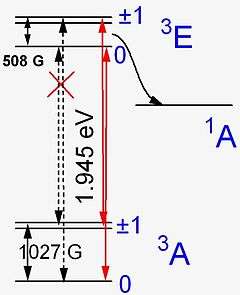
The energy level structure of the N-V− center was established by combining optical, electron paramagnetic resonance and theoretical results, as shown in the figure. In particular, several theoretical works have been done, using the Linear Combination of Atomic Orbitals (LCAO) approach, to build the electronic orbitals to describe the possible quantum states, looking at the N-V center as a molecule. Moreover, group theory results are used, to take into account the symmetry of the diamond crystal, and so the symmetry of the N-V itself. The energy levels are labeled according to the group theory, and in particular are labelled after the irreducible representations of the C3V symmetry group of the defect center, A1, A2 and E. The numbers 3 in 3A and 1 in 1A represent the number of allowable ms spin states, or the spin multiplicity, which range from –S to S for a total of 2S+1 possible states. If S = 1, ms can be −1, 0, or 1. The 1A level is predicted by theory but not directly observed in experiment, and it is believed to play an important role in the quenching of photoluminescence.
In the absence of an external magnetic field, the ground and excited states are split by the magnetic interaction between the two unpaired electrons at the N-V− center (see microscopic model): when two electrons have parallel spins (ms=±1), their energy is higher than when spins are antiparallel (ms=0). The farther apart the electrons are, the weaker their interaction energy D (roughly D ~1/r3).[6] Thus the smaller splitting in the excited state can be viewed in terms of larger electron-electron separation in the excited state. When an external magnetic field is applied to the N-V− center, it does not affect the ms=0 states nor the 1A state (because it has S = 0), but it splits the ms = ±1 levels. If a magnetic field is oriented along the defect axis and reaches about 1027 G (or 508 G) then the ms = –1 and ms = 0 states in the ground (or excited) state become equal in energy; they strongly interact resulting in so-called spin polarization, which strongly affects the intensity of optical absorption and luminescence transitions involving those states.[19]
This happens because transitions between electronic states are mediated by a photon which cannot change overall spin. Thus optical transitions must preserve the total spin and occur between levels of the same total spin. For this reason, transitions 3E↔1A and 1A ↔ 3A are non-radiative and quench the luminescence. Whereas ms = −1 (excited state) ↔ ms = 0 (ground state) transition was forbidden in the absence of an external magnetic field, it becomes allowed when a magnetic field mixes the ms = −1 and ms = 0 levels in the ground state. As a measurable outcome of this phenomenon, luminescence intensity can be strongly modulated by magnetic field.
An important property of the non-radiative transition between 3E and 1A is that it is stronger for ms = ±1 and weaker for ms = 0. This property results in a very useful manipulation of N-V center, which is called optical spin-polarization. First, an off-resonance excitation which has a higher frequency (typically 2.32 eV (532 nm)) than the frequencies of all transitions and thus lays in the vibronic bands for all transitions. By using a pulse of this wavelength, people can excite all spin states and create phonons as well. For a spin state with ms = 0, due to conservation of spin in transition, it will be excited to the corresponding ms = 0 state in 3E and then go back to original state. However, for a spin state with ms = ±1 in 3A, after the excitation, it has a relatively high probability to jump to the intermediate state 1A by non-radiative transition and go to the ground state with ms = 0. After sufficient cycles, the state of the N-V center can be regarded as in the ms = 0 state. Such a process can be used in the initialization of quantum state in quantum information processing.
There is an additional level splitting in the excited 3E state due to the orbital degeneracy and spin-orbit interaction. Importantly, this splitting can be modulated by applying a static electric field,[14][20] in a similar fashion to the magnetic field mechanism outlined above, though the physics of the splitting is somewhat more complex. Nevertheless, an important practical outcome is that the intensity and position of the luminescence lines can be modulated by applying electric or/and magnetic fields.
The energy difference between the ms = 0 and ms = ±1 states corresponds to the microwave region. Thus by irradiating the N-V centers with microwave radiation, one can change the relative population of those levels, thereby again modulating the luminescence intensity.
There is an additional splitting of the ms = ±1 energy levels, which originates from the "hyperfine" interaction between the nuclear and electron spins. Thus finally, the optical absorption and luminescence from the N-V− center consists of roughly a dozen sharp lines with a separation in the MHz-GHz range, and all those lines can be resolved, given proper sample preparation. The intensity and position of those lines can be modulated using the following tools:
- Amplitude and orientation of magnetic field, which splits the ms = ±1 levels in the ground and excited states.
- Amplitude and orientation of elastic field (strain), which can be applied by, e.g., squeezing the diamond. Similar effects can be induced by applying electric field,[14][20] and the electric field can be controlled with much higher precision.
- Continuous-wave microwave radiation, which changes the population of the sublevels within the ground and excited state.[20]
- Tunable laser, which can selectively excite certain sublevels of the ground and excited state.[20][21]
- In addition to those static perturbations, numerous dynamic effects (spin echo, Rabi oscillations, etc.) can be exploited by applying a carefully designed sequence of microwave pulses.[22][23][24][25][26] The first pulse coherently excites the electron spins, and this coherence is then manipulated and probed by the subsequent pulses. Those dynamic effects are rather important for practical realization of quantum computers, which ought to work at high frequency.
It should be noted that the above-described energy structure is by no means exceptional for a defect in diamond or other semiconductor.[27] It was not this structure alone, but a combination of several favorable factors (previous knowledge, easy production and excitation, etc.) which suggested the use of the N-V− center.
Spin dynamics
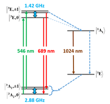
Thinking of the N-V− center as a multielectronic system, we can draw the diagram in the figure at right, where the states are labeled according to their symmetry and with a left superscript that indicates with a 3 if it is a triplet (S=1) and with a 1 if it is a singlet (S=0). It is well accepted today that we have two triplet states and two intermediate singlet states.[31]
The optical excitations conserve the spin state, but there is a high probability of the states decaying non-radiatively to the singlet state , a phenomenon called intersystem crossing (ISC). This happens at an appreciable rate because the energy curve in function of the position of the atoms for the state intersects the curve for the state. Therefore, for some instant during the vibrational relaxation that the ions undergo after the excitement, it is possible for the spin to flip with little or no energy required in the transition.[32] It is important to note that this mechanism also leads to a transition from to , but the rate of this ISC is much lower than the states rate, therefore this transition is indicated with a thin line. The diagram also shows the non-radiative and infrared competing decay paths between the two singlet states, and the fine splitting in the triplet states, whose differences in energy correspond to microwave frequencies.


Some authors explain the dynamics of the N-V− center by admitting that the transition from to is small, but as Robledo et al. shows,[33] only the fact that the probability of decaying to is smaller for than for is enough to polarize the spin to ms = 0.


Potential applications
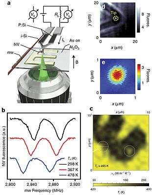
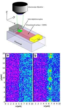
(a) Schematics of experimental setup. An electric current is applied to the arms of an AFM cantilever (phosphorus-doped Si, P:Si) and heats up the end section above the tip (intrinsic Si, i-Si). The bottom lens excites a diamond nanocrystal with a green laser light and collects photoluminescence (PL). The crystal hosts an N-V center and is attached to the AFM tip. A wire on the sample surface serves as the microwave source (mw). The temperature of the cantilever Th is determined from the applied current and voltage.
(b) ODMR spectra of the N-V center at three temperatures. The line splitting originates from a ∼1 mT applied magnetic field.
(c) Thermal conductivity image of a gold letter E on sapphire. White circles indicate features that do not correlate with the AFM topography. (d) PL image of the AFM cantilever end and tip where the diamond nanocrystal appears as the bright spot. (e) Zoomed PL image of the N-V center in d.[34]
The spectral shape and intensity of the optical signals from the N-V− centers are sensitive to external perturbation, such as temperature, strain, electric and magnetic field. However, the use of spectral shape for sensing those perturbation is impractical, as the diamond would have to be cooled to cryogenic temperatures to sharpen the N-V− signals. A more realistic approach is to use luminescence intensity (rather than lineshape), which exhibits a sharp resonance when a microwave frequency is applied to diamond that matches the splitting of the ground state levels. The resulting optically detected magnetic resonance signals are sharp even at room temperature, and can be used in miniature sensors. Such sensors can detect magnetic fields of a few nanotesla[35] or electric fields of about 10 V/cm[36] at kilohertz frequencies after 100 seconds of averaging. This sensitivity allows detecting a magnetic or electric field produced by a single electron located tens of nanometers away from an N-V− center.
Using the same mechanism, the N-V− centers were employed in scanning thermal microscopy to measure high-resolution spatial maps of temperature and thermal conductivity (see image).[34]
Another possible use the N-V− centers is as a detector to measure the full mechanical stress tensor in the bulk of the crystal. For this application, the stress-induced splitting of the zero-phonon-line is exploited, and its polarization properties.[37] A robust frequency-modulated radio receiver using the electron-spin-dependent photoluminescence that operated up to 350 °C demonstrates the possibility for use in extreme conditions.[38]
In addition to the quantum optical applications, luminescence from the N-V− centers can be applied for imaging biological processes, such as fluid flow in living cells.[39] This application relies on good compatibility of diamond nano-particles with the living cells and on favorable properties of photoluminescence from the N-V− centers (strong intensity, easy excitation and detection, temporal stability, etc.). Compared with large single-crystal diamonds, nanodiamonds are cheap (about 1 USD per gram) and available from various suppliers. N-V− centers are produced in diamond powders with sub-micrometre particle size using the standard process of irradiation and annealing described above. Those nanodiamonds are introduced in a cell, and their luminescence is monitored using a standard fluorescence microscope.[40]
Further N-V− center has been hypothesized to be a potential bio-mimetic system for emulating radical pair spin dynamics of the avian compass.[41][42]
Stimulated emission from the N-V− center has been demonstrated, though it could be achieved only from the phonon side-band (i.e. broadband light) and not from the ZPL. For this purpose the center has to be excited at wavelength longer than ~650 nm, as higher-energy excitation ionizes the center.[43]
The first continuous-wave room-temperature maser has been demonstrated.[44][45] It used 532-nm pumped N-V− centers held within a high Purcell factor microwave cavity and an external magnetic field of 4300 G. Continuous maser oscillation generated a coherent signal at ~9.2 GHz.
The N-V center can have a very long spin coherence time approaching the second regime.[46][47] This is advantageous for applications in quantum sensing[48] and quantum communication.[49] Disadvantageous for these applications is the long radiative lifetime (~12 ns) of the N-V center and the strong phonon sideband in its emission spectrum. Both issues can be addressed by putting the N-V center in an optical cavity .
Historical remarks
The microscopic model and most optical properties of ensembles of the N-V− centers have been firmly established in the 1970s based on the optical measurements combined with uniaxial stress[2] and on the electron paramagnetic resonance.[5][6] However, a minor error in EPR results (it was assumed that illumination is required to observe N-V− EPR signals) resulted in the incorrect multiplicity assignments in the energy level structure. In 1991 it was shown that EPR can be observed without illumination,[7] which established the energy level scheme shown above. The magnetic splitting in the excited state has been measured only recently.[19]
The characterization of single N-V− centers has become a very competitive field nowadays, with many dozens of papers published in the most prestigious scientific journals. One of the first results was reported back in 1997.[8] In that paper, it was demonstrated that the fluorescence of single N-V− centers can be detected by room-temperature fluorescence microscopy and that the defect shows perfect photostability. Also one of the outstanding properties of the N-V center was demonstrated, namely room-temperature optically detected magnetic resonance.
See also
| Wikimedia Commons has media related to Nitrogen-vacancy center in diamond. |
References
- 1 2 Schreyvogel, C.; Polyakov, V.; Wunderlich, R.; Meijer, J.; Nebel, C. E. (2015). "Active charge state control of single N-V centres in diamond by in-plane Al-Schottky junctions". Scientific Reports. 5: 12160. Bibcode:2015NatSR...512160S. doi:10.1038/srep12160. PMC 4503995. PMID 26177799.
- 1 2 3 4 Davies, G.; Hamer, M. F. (1976). "Optical Studies of the 1.945 eV Vibronic Band in Diamond". Proceedings of the Royal Society of London A. 348 (1653): 285. Bibcode:1976RSPSA.348..285D. doi:10.1098/rspa.1976.0039.
- ↑ Mita, Y. (1996). "Change of absorption spectra in type-Ib diamond with heavy neutron irradiation". Physical Review B. 53 (17): 11360–11364. Bibcode:1996PhRvB..5311360M. doi:10.1103/PhysRevB.53.11360.
- 1 2 Iakoubovskii, K.; Adriaenssens, G. J.; Nesladek, M. (2000). "Photochromism of vacancy-related centres in diamond" (PDF). Journal of Physics: Condensed Matter. 12 (2): 189. Bibcode:2000JPCM...12..189I. doi:10.1088/0953-8984/12/2/308.
- 1 2 3 Loubser, J. H. N.; van Wyk, J. A. (1977). "Electron Spin Resonance in Annealed Type 1b Diamond". Diamond Research. 11: 4–7. ISSN 0070-4679.
- 1 2 3 4 Loubser, J. H. N.; van Wyk, J. A. (1978). "Electron spin resonance in the study of diamond". Reports on Progress in Physics. 41 (8): 1201. Bibcode:1978RPPh...41.1201L. doi:10.1088/0034-4885/41/8/002.
- 1 2 Redman, D.; Brown, S.; Sands, R.; Rand, S. (1991). "Spin dynamics and electronic states of N-V centers in diamond by EPR and four-wave-mixing spectroscopy". Physical Review Letters. 67 (24): 3420–3423. Bibcode:1991PhRvL..67.3420R. doi:10.1103/PhysRevLett.67.3420. PMID 10044729.
- 1 2 3 4 Gruber, A.; et al. (1997). "Scanning Confocal Optical Microscopy and Magnetic Resonance on Single Defect Centers" (PDF). Science. 276 (5321): 2012–2014. doi:10.1126/science.276.5321.2012.
- ↑ Felton, S.; et al. (2008). "Electron paramagnetic resonance studies of the neutral nitrogen vacancy in diamond". Physical Review B. 77 (8): 081201. Bibcode:2008PhRvB..77h1201F. doi:10.1103/PhysRevB.77.081201.
- ↑ Awschalom, D. D.; Epstein, R.; Hanson, R. (2007). "Diamond Age of Spintronics". Scientific American. 297 (4): 84. Bibcode:2007SciAm.297d..84A. doi:10.1038/scientificamerican1007-84.
- ↑ Lang, A. R.; et al. (1991). "On the Dilatation of Synthetic Type Ib Diamond by Substitutional Nitrogen Impurity". Philosophical Transactions of the Royal Society A. 337 (1648): 497–520. Bibcode:1991RSPTA.337..497L. doi:10.1098/rsta.1991.0135.
- ↑ Iakoubovskii, K.; Adriaenssens, G. J. (2001). "Trapping of vacancies by defects in diamond". Journal of Physics: Condensed Matter. 13 (26): 6015. Bibcode:2001JPCM...13.6015I. doi:10.1088/0953-8984/13/26/316.
- ↑ Edmonds, A.; d’Haenens-Johansson, U.; Cruddace, R.; Newton, M.; Fu, K. -M.; Santori, C.; Beausoleil, R.; Twitchen, D.; Markham, M. (2012). "Production of oriented nitrogen-vacancy color centers in synthetic diamond". Physical Review B. 86 (3): 035201. arXiv:1112.5757. Bibcode:2012PhRvB..86c5201E. doi:10.1103/PhysRevB.86.035201.
- 1 2 3 Tamarat, Ph.; et al. (2006). "Stark Shift Control of Single Optical Centers in Diamond". Physical Review Letters. 97 (8): 083002. arXiv:quant-ph/0607170. Bibcode:2006PhRvL..97h3002T. doi:10.1103/PhysRevLett.97.083002. PMID 17026299.
- 1 2 Kuhn, S.; et al. (2001). "Diamond colour centres as a nanoscopic light source for scanning near-field optical microscopy". Journal of Microscopy. 202 (1): 2–6. doi:10.1046/j.1365-2818.2001.00829.x. PMID 11298860.
- ↑ De Weerdt, F.; Collins, A. T.; Zugik, M.; Connor, A. (2005). "Sub-threshold excitation of luminescene of defects in diamonds". Journal of Physics: Condensed Matter. 50 (17): 8005. Bibcode:2005JPCM...17.8005D. doi:10.1088/0953-8984/17/50/018.
- ↑ Collins, A. T.; Thomaz, M. F.; Jorge, M. I. B. (1983). "Luminescence decay time of the 1.945 eV centre in type Ib diamond". Journal of Physics C. 16 (11): 2177. Bibcode:1983JPhC...16.2177C. doi:10.1088/0022-3719/16/11/020.
- ↑ Hanzawa, H.; Nisida, Y.; Kato, T. (1997). "Measurement of decay time for the NV centre in Ib diamond with a picosecond laser pulse". Diamond and Related Materials. 6 (11): 1595. Bibcode:1997DRM.....6.1595H. doi:10.1016/S0925-9635(97)00037-X.
- 1 2 3 Fuchs, G. D.; et al. (2008). "Excited-State Spectroscopy Using Single Spin Manipulation in Diamond". Physical Review Letters. 101 (1): 117601. arXiv:0806.1939. Bibcode:2008PhRvL.101k7601F. doi:10.1103/PhysRevLett.101.117601. PMID 18851332.
- 1 2 3 4 Tamarat, Ph.; et al. (2008). "Spin-flip and spin-conserving optical transitions of the nitrogen-vacancy centre in diamond". New Journal of Physics. 10 (4): 045004. Bibcode:2008NJPh...10d5004T. doi:10.1088/1367-2630/10/4/045004.
- ↑ Santori, C.; et al. (2006). "Coherent Population Trapping of Single Spins in Diamond under Optical Excitation". Physical Review Letters. 97 (24): 247401. arXiv:quant-ph/0607147. Bibcode:2006PhRvL..97x7401S. doi:10.1103/PhysRevLett.97.247401. hdl:2318/103560. PMID 17280321.
- ↑ Hanson, R.; Gywat, O.; Awschalom, D. D. (2006). "Room-temperature manipulation and decoherence of a single spin in diamond". Physical Review B. 74 (16): 161203. arXiv:quant-ph/0608233. Bibcode:2006PhRvB..74p1203H. doi:10.1103/PhysRevB.74.161203.
- ↑ Dutt, M. V. G.; et al. (2007). "Quantum Register Based on Individual Electronic and Nuclear Spin Qubits in Diamond" (PDF). Science. 316 (5829): 1312–6. Bibcode:2007Sci...316.....D. doi:10.1126/science.1139831. PMID 17540898.
- ↑ Childress, L.; et al. (2006). "Coherent Dynamics of Coupled Electron and Nuclear Spin Qubits in Diamond". Science. 314 (5797): 281–5. Bibcode:2006Sci...314..281C. doi:10.1126/science.1131871. PMID 16973839.
- ↑ Batalov, A.; et al. (2008). "Temporal Coherence of Photons Emitted by Single Nitrogen-Vacancy Defect Centers in Diamond Using Optical Rabi-Oscillations" (PDF). Physical Review Letters. 100 (7): 077401. Bibcode:2008PhRvL.100g7401B. doi:10.1103/PhysRevLett.100.077401. hdl:11858/00-001M-0000-0011-A088-E. PMID 18352594.
- ↑ Jelezko, F.; et al. (2004). "Observation of Coherent Oscillations in a Single Electron Spin" (PDF). Physical Review Letters. 92 (7): 076401. Bibcode:2004PhRvL..92g6401J. doi:10.1103/PhysRevLett.92.076401. PMID 14995873.
- ↑ Aharonovich, I.; et al. (2009). "Enhanced single-photon emission in the near infrared from a diamond color center". Physical Review B. 79 (23): 235316. Bibcode:2009PhRvB..79w5316A. doi:10.1103/PhysRevB.79.235316.
- ↑ Gordon, Luke; Weber, Justin R.; Varley, Joel B.; Janotti, Anderson; Awschalom, David D.; Van de Walle, Chris G. (2013-10-01). "Quantum computing with defects". MRS Bulletin. 38 (10): 802–807. doi:10.1557/mrs.2013.206. PMC 2889300. PMID 20404195.
- ↑ Rogers, L. J.; Doherty, M. W.; Barson, M. S. J.; Onoda, S.; Ohshima, T.; Manson, N. B. (2015-01-01). "Singlet levels of the NV − centre in diamond". New Journal of Physics. 17 (1): 013048. arXiv:1407.6244. Bibcode:2015NJPh...17a3048R. doi:10.1088/1367-2630/17/1/013048.
- ↑ Rogers, L. J.; Armstrong, S.; Sellars, M. J.; Manson, N. B. (2008). "Infrared emission of the NV centre in diamond: Zeeman and uniaxial stress studies". New Journal of Physics. 10 (10): 103024. doi:10.1088/1367-2630/10/10/103024. ISSN 1367-2630.
- ↑ Doherty, Marcus W.; Manson, Neil B.; Delaney, Paul; Jelezko, Fedor; Wrachtrup, Jörg; Hollenberg, Lloyd C. L. (2013-07-01). "The nitrogen-vacancy colour centre in diamond". Physics Reports. The nitrogen-vacancy colour centre in diamond. 528 (1): 1–45. arXiv:1302.3288. Bibcode:2013PhR...528....1D. CiteSeerX 10.1.1.743.9147. doi:10.1016/j.physrep.2013.02.001.
- ↑ Choi, SangKook (2012-01-01). "Mechanism for optical initialization of spin in NV". Physical Review B. 86 (4): 041202. Bibcode:2012PhRvB..86d1202C. doi:10.1103/PhysRevB.86.041202.
- ↑ Robledo, Lucio; Bernien, Hannes; Sar, Toeno van der; Hanson, Ronald (2011-01-01). "Spin dynamics in the optical cycle of single nitrogen-vacancy centres in diamond". New Journal of Physics. 13 (2): 025013. arXiv:1010.1192. Bibcode:2011NJPh...13b5013R. doi:10.1088/1367-2630/13/2/025013.
- 1 2 Laraoui, Abdelghani; Aycock-Rizzo, Halley; Gao, Yang; Lu, Xi; Riedo, Elisa; Meriles, Carlos A. (2015). "Imaging thermal conductivity with nanoscale resolution using a scanning spin probe". Nature Communications. 6 (8954): 8954. arXiv:1511.06916. Bibcode:2015NatCo...6E8954L. doi:10.1038/ncomms9954. PMC 4673876. PMID 26584676.
- ↑ Maze, J. R.; Stanwix, P. L.; Hodges, J. S.; Hong, S.; Taylor, J. M.; Cappellaro, P.; Jiang, L.; Dutt, M. V. G.; Togan, E.; Zibrov, A. S.; Yacoby, A.; Walsworth, R. L.; Lukin, M. D. (2008). "Nanoscale magnetic sensing with an individual electronic spin in diamond" (PDF). Nature. 455 (7213): 644–647. Bibcode:2008Natur.455..644M. doi:10.1038/nature07279. PMID 18833275.
- ↑ Dolde, F.; Fedder, H.; Doherty, M. W.; Nöbauer, T.; Rempp, F.; Balasubramanian, G.; Wolf, T.; Reinhard, F.; Hollenberg, L. C. L.; Jelezko, F.; Wrachtrup, J. (2011). "Electric-field sensing using single diamond spins". Nature Physics. 7 (6): 459. arXiv:1103.3432. Bibcode:2011NatPh...7..459D. doi:10.1038/nphys1969. hdl:11858/00-001M-0000-0027-768E-1.
- ↑ Grazioso, F.; Patton, B. R.; Delaney, P.; Markham, M. L.; Twitchen, D. J.; Smith, J. M. (2013). "Measurement of the full stress tensor in a crystal using photoluminescence from point defects: The example of nitrogen vacancy centers in diamond". Applied Physics Letters. 103 (10): 101905. arXiv:1110.3658. Bibcode:2013ApPhL.103j1905G. doi:10.1063/1.4819834.
- ↑ Shao, Linbo; Zhang, Mian; Markham, Matthew; Edmonds, Andrew; Loncar, Marko (15 December 2016). "Diamond Radio Receiver: Nitrogen-Vacancy Centers as Fluorescent Transducers of Microwave Signals". Phys. Rev. Appl. 6 (6): 064008. Bibcode:2016PhRvP...6f4008S. doi:10.1103/PhysRevApplied.6.064008.
- ↑ Chang, Y.-R.; et al. (2008). "Mass production and dynamic imaging of fluorescent nanodiamonds" (PDF). Nature Nanotechnology. 3 (5): 284–8. doi:10.1038/nnano.2008.99. PMID 18654525.
- ↑ Aharonovich, I.; Greentree, A. D.; Prawer, S. (2011). "Diamond photonics". Nature Photonics. 5 (7): 397. Bibcode:2011NaPho...5..397A. doi:10.1038/nphoton.2011.54.
- ↑ Cryptochrome and Magnetic Sensing, University of Illinois at Urbana-Champaign
- ↑ Cai, Jianming; Guerreschi, Gian Giacomo; Briegel, Hans J. (2010-06-04). "Quantum Control and Entanglement in a Chemical Compass". Physical Review Letters. 104 (22): 220502. arXiv:0906.2383. Bibcode:2010PhRvL.104v0502C. doi:10.1103/PhysRevLett.104.220502. PMID 20867156.
- ↑ Jeske, Jan; Lau, Desmond W. M.; Vidal, Xavier; McGuinness, Liam P.; Reineck, Philipp; Johnson, Brett C.; Doherty, Marcus W.; McCallum, Jeffrey C.; Onoda, Shinobu; Jelezko, Fedor; Ohshima, Takeshi; Volz, Thomas; Cole, Jared H.; Gibson, Brant C.; Greentree, Andrew D. (2017). "Stimulated emission from nitrogen-vacancy centres in diamond". Nature Communications. 8: 14000. arXiv:1602.07418. Bibcode:2017NatCo...814000J. doi:10.1038/ncomms14000. PMC 5290152. PMID 28128228.
- ↑ Breeze, Jonathan D.; Sathian, Juna; Salvadori, Enrico; Alford, Neil McN; Kay, Christopher W. M. (2018-03-21). "Continuous-wave room-temperature diamond maser". Nature. 555 (7697): 493–496. arXiv:1710.07726. Bibcode:2018Natur.555..493B. doi:10.1038/nature25970. ISSN 0028-0836. PMID 29565362.
- ↑ Liu, Ren-Bao (22 March 2018). "A diamond age of masers". Nature. 555 (7697): 447–449. doi:10.1038/d41586-018-03215-3. PMID 29565370.
- ↑ Maurer, P.C.; Kucsko, G.; Latta, C.; Jiang, L.; Yao, N.Y.; Bennett, S.D.; Pastawski, F.; Hunger, D.; Chisholm, N.; Markham, M.; Twitchen, D.J.; Cirac, J.I.; Lukin, M.D. (2012). "Room-temperature quantum bit memory exceeding one second" (Submitted manuscript). Science. 336 (6086): 1283–1286. Bibcode:2012Sci...336.1283M. doi:10.1126/science.1220513. PMID 22679092.
- ↑ Bar-Gill, N.; Pham, L.M.; Jarmola, A.; Budker, D.; Walsworth, R.L. (2012). "Solid-state electronic spin coherence time approaching one second". Nature Communications. 4: 1743. arXiv:1211.7094. Bibcode:2013NatCo...4E1743B. doi:10.1038/ncomms2771. PMID 23612284.
- ↑ Mamin, H. J.; Kim, M.; Sherwood, M. H.; Rettner, C. T.; Ohno, K.; Awschalom, D. D.; Rugar, D. (2013). "Nanoscale Nuclear Magnetic Resonance with a Nitrogen-Vacancy Spin Sensor". Science. 339 (6119): 557–560. Bibcode:2013Sci...339..557M. doi:10.1126/science.1231540. PMID 23372008.
- ↑ Hensen, B.; Bernien, H.; Dréau, A.E.; Reiserer, A.; Kalb, N.; Blok, M.S.; Ruitenberg, J.; Vermeulen, R.F.; Schouten, R.N.; Abellán, C.; Amaya, W.; Pruneri, V.; Mitchell, M.W.; Markham, M.; Twitchen, D.J.; Elkouss, D.; Wehner, S.; Taminiau, T.H.; Hanson, R. (2015). "Loophole-free Bell inequality violation using electron spins separated by 1.3 kilometres". Nature. 526 (7575): 682–686. arXiv:1508.05949. Bibcode:2015Natur.526..682H. doi:10.1038/nature15759. PMID 26503041.
| General |  | ||||||||
|---|---|---|---|---|---|---|---|---|---|
| Quantum communication | |||||||||
| Quantum algorithms | |||||||||
| Quantum complexity theory | |||||||||
| Quantum computing models | |||||||||
| Quantum error correction | |||||||||
| Physical implementations |
| ||||||||
| Software | |||||||||