Jacobs Institute for Design Innovation
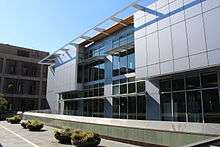
The Jacobs Institute for Design Innovation is a building on the UC Berkeley campus, part of the UC Berkeley College of Engineering. Construction began in August 2014 with a $20 million gift from the Paul and Stacy Jacobs Foundation.[1] The ribbon-cutting ceremony took place on August 20, 2015, with speeches by speeches by various UC Berkeley administrators, Ellen Lupton,[2] Paul E. Jacobs, executive chairman of Qualcomm,[3] and the building opened for instruction on September 16. The 24,000-square-foot building was constructed at a cost of $25 million, funded by philanthropy.
The building includes open student studio space on the first floor, two classrooms on the second floor, and a large conference room on the third floor.[4] It has design studios with shop tools and rapid prototyping equipment.[5]
External links
References
- ↑ "UC Berkeley's new Jacobs Hall to open in fall". The Daily Californian. Retrieved 25 November 2015.
- ↑ "News & Events". Jacobs Institute.
- ↑ "Grand opening for Jacobs Hall, the new hub for all things design". Berkeley News. Retrieved 25 November 2015.
- ↑
- ↑ Mathew, Teresa (2015-08-26). "$24M UC Berkeley innovation institute partners with companies to boost maker movement". San Francisco Business Times. Retrieved 2015-12-25.
Located in: Berkeley, California | |||||||||
| Academics |
|  | |||||||
| Athletics |
| ||||||||
| Campus |
| ||||||||
| Research | |||||||||
| Organizations | |||||||||
| Related articles | |||||||||
| |||||||||
Coordinates: 37°52′34″N 122°15′32″W / 37.876022°N 122.258802°W