High Bandwidth Memory

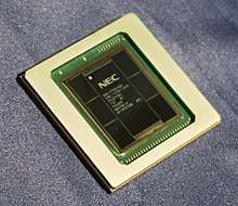
High Bandwidth Memory (HBM) is a high-performance RAM interface for 3D-stacked DRAM from Samsung, AMD and Hynix. It is to be used in conjunction with high-performance graphics accelerators and network devices.[1] The first devices to use HBM are the AMD Fiji GPUs.[2][3]
High Bandwidth Memory has been adopted by JEDEC as an industry standard in October 2013.[4] The second generation, HBM2, was accepted by JEDEC in January 2016.[5]
Technology
HBM achieves higher bandwidth while using less power in a substantially smaller form factor than DDR4 or GDDR5.[6] This is achieved by stacking up to eight DRAM dies, including an optional base die with a memory controller, which are interconnected by through-silicon vias (TSV) and microbumps. The HBM technology is similar in principle but incompatible with the Hybrid Memory Cube interface developed by Micron Technology.[7]
HBM memory bus is very wide in comparison to other DRAM memories such as DDR4 or GDDR5. An HBM stack of four DRAM dies (4-Hi) has two 128-bit channels per die for a total of 8 channels and a width of 1024 bits in total. A graphics card/GPU with four 4-Hi HBM stacks would therefore have a memory bus with a width of 4096 bits. In comparison, the bus width of GDDR memories is 32 bits, with 16 channels for a graphics card with a 512-bit memory interface.[8] HBM supports up to 4 GB per package.
The larger number of connections to the memory, relative to DDR4 or GDDR5, required a new method of connecting the HBM memory to the GPU (or other processor).[9] AMD and Nvidia have both used purpose built silicon chips, called interposers, to connect the memory and GPU. This interposer has the added advantage of requiring the memory and processor to be physically close, decreasing memory paths. However, as semiconductor device fabrication is significantly more expensive than printed circuit board manufacture, this adds cost to the final product.
Interface
The HBM DRAM is tightly coupled to the host compute die with a distributed interface. The interface is divided into independent channels. Each channel is completely independent of one another. Channels are not necessarily synchronous to each other. The HBM DRAM uses a wide-interface architecture to achieve high-speed, low-power operation. The HBM DRAM uses a 500 MHz differential clock CK_t/CK_c. Commands are registered at the rising edge of CK_t, CK_c. Each channel interface maintains a 128 bit data bus operating at DDR data rates. HBM supports transfer rates of 1 GT/s per pin (transferring 1 bit), yielding an overall package bandwidth of 128 GB/s.[10]
HBM 2
The second generation of High Bandwidth Memory, HBM 2, also specifies up to eight dies per stack and doubles pin transfer rates up to 2 GT/s. Retaining 1024-bit wide access, HBM2 is able to reach 256 GB/s memory bandwidth per package. The HBM2 spec allows up to 8 GB per package. HBM2 is predicted to be especially useful for performance-sensitive consumer applications such as virtual reality.[11]
On January 19, 2016, Samsung announced early mass production of HBM2, at up to 8 GB per stack.[12][13] SK Hynix also announced availability of 4 GB stacks in August 2016.[14]
HBM 3
A third generation of High Bandwidth Memory, HBM 3, was announced in 2016.[15][16] HBM3 is expected to offer increased memory capacity, greater bandwidth, lower voltage, and lower costs. The increased density is expected to come from greater density per die and more die stacks per chip. Bandwidth is expected to be 512 GB/s or greater. No release date has been announced, though Samsung expects volume production by 2020.
HBM 4
For the future of Exascale high-performance computers, HPE predicts OPGHC HBM3+ and HBM4 to be released between 2022 and 2024. More stacking and higher capacity should bring more memory per socket and higher speed. HBM 3+ is planned with 4 TB/s and 1024 GB per socket. (For comparison, High-end AMD EPYC chips have 150 GB/s and 2000 GB RAM per socket.)[17]
History
The development of High Bandwidth Memory began at AMD in 2008 to solve the problem of ever increasing power usage and form factor of computer memory. Amongst other things AMD developed procedures to solve the die stacking problems with a team led by Senior AMD Fellow Bryan Black. Partners from the memory industry (SK Hynix), interposer industry (UMC) and packaging industry (Amkor Technology and ASE) were obtained to help AMD realize their vision of HBM.[18] High volume manufacturing began at a Hynix facility in Icheon, Korea in 2015.
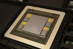
HBM has been adopted as industry standard JESD235 by JEDEC as of October 2013 following a proposal by AMD and SK Hynix in 2010.[4] The first GPU utilizing HBM is AMD Fiji which was released in June 2015 powering the AMD Radeon R9 Fury X.[19][2][20]
HBM2 was accepted by JEDEC as standard JESD235a in January 2016.[5] The first GPU chip utilizing HBM2 is the Nvidia Tesla P100 which was officially announced in April 2016.[21][22]
Future
At Hot Chips in August 2016 both Samsung and Hynix announced the next generation HBM memory technologies.[23][24] Both companies announced high performance products expected to have increased density, increased bandwidth, and lower power. Samsung also announced a lower cost version of HBM under development targeting mass markets. Removing the buffer die and decreasing the number of TSVs lowers cost, though at the expense of a decreased overall bandwidth (200 GB/s).
See also
- Stacked DRAM
- Chip stack multi-chip modules
- Hybrid Memory Cube stacked memory standard from Micron (2011)
References
- ↑ ISSCC 2014 Trends Archived 2015-02-06 at the Wayback Machine. page 118 "High-Bandwidth DRAM"
- 1 2 Smith, Ryan (2 July 2015). "The AMD Radeon R9 Fury X Review". Anandtech. Retrieved 1 August 2016.
- ↑ Morgan, Timothy Prickett (March 25, 2014). "Future Nvidia 'Pascal' GPUs Pack 3D Memory, Homegrown Interconnect". EnterpriseTech. Retrieved 26 August 2014.
Nvidia will be adopting the High Bandwidth Memory (HBM) variant of stacked DRAM that was developed by AMD and Hynix
- 1 2 HIGH BANDWIDTH MEMORY (HBM) DRAM (JESD235), JEDEC, October 2013
- 1 2 "JESD235a: High Bandwidth Memory 2". 2016-01-12.
- ↑ HBM: Memory Solution for Bandwidth-Hungry Processors Archived 2015-04-24 at the Wayback Machine., Joonyoung Kim and Younsu Kim, SK hynix // Hot Chips 26, August 2014
- ↑ Where Are DRAM Interfaces Headed? // EETimes, 4/18/2014 "The Hybrid Memory Cube (HMC) and a competing technology called High-Bandwidth Memory (HBM) are aimed at computing and networking applications. These approaches stack multiple DRAM chips atop a logic chip."
- ↑ Highlights of the HighBandwidth Memory (HBM) Standard. Mike O’Connor, Sr. Research Scientist, NVidia // The Memory Forum – June 14, 2014
- ↑ Smith, Ryan (19 May 2015). "AMD Dives Deep On High Bandwidth Memory - What Will HBM Bring to AMD?". Anandtech. Retrieved 12 May 2017.
- ↑ "High-Bandwidth Memory (HBM)" (PDF). AMD. 2015-01-01. Retrieved 2016-08-10.
- ↑ Valich, Theo. "NVIDIA Unveils Pascal GPU: 16GB of memory, 1TB/s Bandwidth". VR World. Retrieved 2016-01-24.
- ↑ "Samsung Begins Mass Producing World's Fastest DRAM – Based on Newest High Bandwidth Memory (HBM) Interface". news.samsung.com.
- ↑ "Samsung announces mass production of next-generation HBM2 memory - ExtremeTech". 19 January 2016.
- ↑ Shilov, Anton (1 August 2016). "SK Hynix Adds HBM2 to Catalog". Anandtech. Retrieved 1 August 2016.
- ↑ Walton, Mark (23 August 2016). "HBM3: Cheaper, up to 64GB on-package, and terabytes-per-second bandwidth". Ars Technica. Retrieved 3 February 2017.
- ↑ Ferriera, Bruno (23 August 2016). "HBM3 and GDDR6 emerge fresh from the oven of Hot Chips". Tech Report. Retrieved 3 February 2017.
- ↑ https://www.computerbase.de/2018-03/ddr-hbm3-hbm4-ram/
- ↑ High-Bandwidth Memory (HBM) from AMD: Making Beautiful Memory
- ↑ Smith, Ryan (19 May 2015). "AMD HBM Deep Dive". Anandtech. Retrieved 1 August 2016.
- ↑ AMD Ushers in a New Era of PC Gaming including World’s First Graphics Family with Revolutionary HBM Technology
- ↑ Smith, Ryan (5 April 2016). "Nvidia announces Tesla P100 Accelerator". Anandtech. Retrieved 1 August 2016.
- ↑ "NVIDIA Tesla P100: The Most Advanced Data Center GPU Ever Built". www.nvidia.com.
- ↑ Smith, Ryan (23 August 2016). "Hot Chips 2016: Memory Vendors Discuss Ideas for Future Memory Tech - DDR5, Cheap HBM & More". Anandtech. Retrieved 23 August 2016.
- ↑ Walton, Mark (23 August 2016). "HBM3: Cheaper, up to 64GB on-package, and terabytes-per-second bandwidth". Ars Technica. Retrieved 23 August 2016.
External links
- HIGH BANDWIDTH MEMORY (HBM) DRAM (JESD235), JEDEC, October 2013
- 25.2 A 1.2V 8Gb 8-channel 128GB/s high-bandwidth memory (HBM) stacked DRAM with effective microbump I/O test methods using 29 nm process and TSV. D.U Lee, SK hynix, ISSCC 2014 doi:10.1109/ISSCC.2014.6757501
- HBM vs HBM2 vs GDDR5 vs GDDR5X Memory Comparison