Gallium nitride
 | |
 | |
| Names | |
|---|---|
| IUPAC name
Gallium nitride | |
| Identifiers | |
3D model (JSmol) |
|
| ChemSpider | |
| ECHA InfoCard | 100.042.830 |
PubChem CID |
|
| RTECS number | LW9640000 |
| |
| |
| Properties | |
| GaN | |
| Molar mass | 83.730 g/mol[1] |
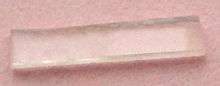
| Appearance | yellow powder |
| Density | 6.1 g/cm3[1] |
| Melting point | >2500 °C[1][2] |
| Insoluble[3] | |
| Band gap | 3.4 eV (300 K, direct) |
| Electron mobility | 1500 cm2/(V·s) (300 K)[4] |
| Thermal conductivity | 1.3 W/(cm·K) (300 K)[5] |
Refractive index (nD) |
2.429 |
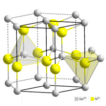
| Structure | |
| Wurtzite | |
| C6v4-P63mc | |
| Tetrahedral | |
| Thermochemistry | |
Std enthalpy of formation (ΔfH |
−110.2 kJ/mol[7] |
| Hazards | |
| Flash point | Non-flammable |
| Related compounds | |
Other anions |
Gallium phosphide Gallium arsenide Gallium antimonide |
Other cations |
Boron nitride Aluminium nitride Indium nitride |
Related compounds |
Aluminium gallium arsenide Indium gallium arsenide Gallium arsenide phosphide Aluminium gallium nitride Indium gallium nitride |
Except where otherwise noted, data are given for materials in their standard state (at 25 °C [77 °F], 100 kPa). | |
| Infobox references | |
Gallium nitride (GaN) is a binary III/V direct bandgap semiconductor commonly used in light-emitting diodes since the 1990s. The compound is a very hard material that has a Wurtzite crystal structure. Its wide band gap of 3.4 eV affords it special properties for applications in optoelectronic,[8][9] high-power and high-frequency devices. For example, GaN is the substrate which makes violet (405 nm) laser diodes possible, without use of nonlinear optical frequency-doubling.
Its sensitivity to ionizing radiation is low (like other group III nitrides), making it a suitable material for solar cell arrays for satellites. Military and space applications could also benefit as devices have shown stability in radiation environments.[10]
Because GaN transistors can operate at much higher temperatures and work at much higher voltages than gallium arsenide (GaAs) transistors, they make ideal power amplifiers at microwave frequencies. In addition, GaN offers promising characteristics for THz devices.[11]
Physical properties

GaN is a very hard (12±2 GPa[12]:4), mechanically stable wide bandgap semiconductor material with high heat capacity and thermal conductivity.[13] In its pure form it resists cracking and can be deposited in thin film on sapphire or silicon carbide, despite the mismatch in their lattice constants.[13] GaN can be doped with silicon (Si) or with oxygen[14] to n-type and with magnesium (Mg) to p-type.[15] However, the Si and Mg atoms change the way the GaN crystals grow, introducing tensile stresses and making them brittle.[16] Gallium nitride compounds also tend to have a high dislocation density, on the order of 108 to 1010 defects per square centimeter.[17] The wide band-gap behavior of GaN is connected to specific changes in the electronic band structure, charge occupation and chemical bond regions.[18]
Developments
GaN with a high crystalline quality can be obtained by depositing a buffer layer at low temperatures.[19] Such high-quality GaN led to the discovery of p-type GaN,[15] p-n junction blue/UV-LEDs[15] and room-temperature stimulated emission[20] (essential for laser action).[21] This has led to the commercialization of high-performance blue LEDs and long-lifetime violet-laser diodes, and to the development of nitride-based devices such as UV detectors and high-speed field-effect transistors.
LEDs
High-brightness GaN light-emitting diodes (LEDs) completed the range of primary colors, and made applications such as daylight visible full-color LED displays, white LEDs and blue laser devices possible. The first GaN-based high-brightness LEDs used a thin film of GaN deposited via Metal-Organic Vapour Phase Epitaxy (MOVPE) on sapphire. Other substrates used are zinc oxide, with lattice constant mismatch of only 2% and silicon carbide (SiC).[22] Group III nitride semiconductors are, in general, recognized as one of the most promising semiconductor families for fabricating optical devices in the visible short-wavelength and UV region.
Transistors
The very high breakdown voltages,[23] high electron mobility and saturation velocity of GaN has also made it an ideal candidate for high-power and high-temperature microwave applications, as evidenced by its high Johnson's figure of merit. Potential markets for high-power/high-frequency devices based on GaN include microwave radio-frequency power amplifiers (such as those used in high-speed wireless data transmission) and high-voltage switching devices for power grids. A potential mass-market application for GaN-based RF transistors is as the microwave source for microwave ovens, replacing the magnetrons currently used. The large band gap means that the performance of GaN transistors is maintained up to higher temperatures (~400 °C[24]) than silicon transistors (~150 °C[24]) because it lessens the effects of thermal generation of charge carriers that are inherent to any semiconductor. The first gallium nitride metal semiconductor field-effect transistors (GaN MESFET) were experimentally demonstrated in 1993[25] and they are being actively developed.
In 2010 the first enhancement-mode GaN transistors became generally available.[26] Only n-channel transistors were available.[26] These devices were designed to replace power MOSFETs in applications where switching speed or power conversion efficiency is critical. These transistors, also called eGaN FETs, are built by growing a thin layer of GaN on top of a standard silicon wafer. This allows the eGaN FETs to maintain costs similar to silicon power MOSFETs but with the superior electrical performance of GaN.
Applications
LEDs
GaN-based violet laser diodes are used to read Blu-ray Discs. The mixture of GaN with In (InGaN) or Al (AlGaN) with a band gap dependent on ratio of In or Al to GaN allows the manufacture of light-emitting diodes (LEDs) with colors that can go from red to ultra-violet.[22]
Transistors
GaN transistors are suitable for high frequency, high voltage, high temperature and high efficiency applications.
GaN HEMTs have been offered commercially since 2006, and have found immediate use in various wireless infrastructure applications due to their high efficiency and high voltage operation. A second generation of devices with shorter gate lengths will address higher frequency telecom and aerospace applications.[27]
GaN based MOSFET and MESFET transistors also offer advantages including lower loss in high power electronics, especially in automotive and electric car applications.[28] Since 2008 these can be formed on a silicon substrate.[28] High-voltage (800 V) Schottky barrier diodes (SBDs) have also been made.[28]
They are also utilized in military electronics such as active electronically scanned array radars.[29]
GaN-based electronics (not pure GaN) has the potential to drastically cut energy consumption, not only in consumer applications but even for power transmission utilities.
Unlike silicon transistors which switch off due to power surges, GaN transistors are typically depletion mode devices (i.e. on / resistive when the gate-source voltage is zero). Several methods have been proposed to reach normally-off (or E-mode) operation, which is necessary for use in power electronics:[30][31]
- the implantation of fluorine ions under the gate (the negative charge of the F-ions favors the depletion of the channel)
- the use of a MIS-type gate stack, with recess of the AlGaN
- the integration of a cascoded pair constituted by a normally-on GaN transistor and a low voltage silicon MOSFET
- the use of a p-type layer on top of the AlGaN/GaN heterojunction
Nanoscale
GaN nanotubes are proposed for applications in nanoscale electronics, optoelectronics and biochemical-sensing applications.[32]
Spintronics potential
When doped with a suitable transition metal such as manganese, GaN is a promising spintronics material (magnetic semiconductors).[22]
Synthesis
Bulk substrates
GaN crystals can be grown from a molten Na/Ga melt held under 100 atmospheres of pressure of N2 at 750 °C. As Ga will not react with N2 below 1000 °C, the powder must be made from something more reactive, usually in one of the following ways:
Gallium nitride can also be synthesized by injecting ammonia gas into molten gallium at 900-980 °C at normal atmospheric pressure.[35]
Molecular beam epitaxy
Commercially, GaN crystals can be grown using molecular beam epitaxy or metalorganic vapour phase epitaxy. This process can be further modified to reduce dislocation densities. First, an ion beam is applied to the growth surface in order to create nanoscale roughness. Then, the surface is polished. This process takes place in a vacuum.
Safety
GaN dust is an irritant to skin, eyes and lungs. The environment, health and safety aspects of gallium nitride sources (such as trimethylgallium and ammonia) and industrial hygiene monitoring studies of MOVPE sources have been reported recently in a review.[36]
Bulk GaN is non-toxic and biocompatible.[37] Therefore, it may be used in the electrodes and electronics of implants in living organisms.
See also
References
- 1 2 3 Haynes, William M., ed. (2011). CRC Handbook of Chemistry and Physics (92nd ed.). Boca Raton, FL: CRC Press. p. 4.64. ISBN 1439855110.
- ↑ Harafuji, Kenji; Tsuchiya, Taku; Kawamura, Katsuyuki (2004). "Molecular dynamics simulation for evaluating melting point of wurtzite-type GaN crystal". Appl. Phys. 96 (5): 2501. Bibcode:2004JAP....96.2501H. doi:10.1063/1.1772878.
- ↑ "abstract NCSU study: Aqueous Stability of Ga- and N-Polar Gallium Nitride".
- ↑ Johan Strydom; Michael de Rooij; David Reusch; Alex Lidow (2015). GaN Transistors for efficient power conversion (2 ed.). California, USA: Wiley. p. 3. ISBN 978-1-118-84479-3.
- ↑ Mion, Christian (2005). "Investigation of the Thermal Properties of Gallium Nitride Using the Three Omega Technique", Thesis, North Carolina State University.
- ↑ Bougrov V., Levinshtein M.E., Rumyantsev S.L., Zubrilov A., in Properties of Advanced Semiconductor Materials GaN, AlN, InN, BN, SiC, SiGe. Eds. Levinshtein M.E., Rumyantsev S.L., Shur M.S., John Wiley & Sons, Inc., New York, 2001, 1–30
- ↑ Haynes, William M., ed. (2011). CRC Handbook of Chemistry and Physics (92nd ed.). Boca Raton, FL: CRC Press. p. 5.12. ISBN 1439855110.
- ↑ Di Carlo, A. (2001). "Tuning Optical Properties of GaN-Based Nanostructures by Charge Screening". Physica Status Solidi A. 183: 81–85. Bibcode:2001PSSAR.183...81D. doi:10.1002/1521-396X(200101)183:1<81::AID-PSSA81>3.0.CO;2-N.
- ↑ Arakawa, Y. (2002). "Progress in GaN-based quantum dots for optoelectronics applications". IEEE Journal of Selected Topics in Quantum Electronics. 8 (4): 823–832. Bibcode:2002IJSTQ...8..823A. doi:10.1109/JSTQE.2002.801675.
- ↑ Lidow, Alexander; Witcher, J. Brandon; Smalley, Ken (March 2011). "Enhancement Mode Gallium Nitride (eGaN) FET Characteristics under Long Term Stress" (PDF). GOMAC Tech Conference.
- ↑ Ahi, Kiarash (September 2017). "Review of GaN-based devices for terahertz operation". Optical Engineering. 56: 090901 – via SPIE.
- ↑ Gallium Nitride as an Electromechanical Material. R-Z. IEEE 2014
- 1 2 Akasaki, I.; Amano, H. (1997). "Crystal Growth and Conductivity Control of Group III Nitride Semiconductors and Their Application to Short Wavelength Light Emitters". Japanese Journal of Applied Physics. 36: 5393. Bibcode:1997JaJAP..36.5393A. doi:10.1143/JJAP.36.5393.
- ↑ Wetzel, C.; Suski, T.; Ager, J.W. III; Fischer, S.; Meyer, B.K.; Grzegory, I.; Porowski, S. (1996) Strongly localized donor level in oxygen doped gallium nitride, International conference on physics of semiconductors, Berlin (Germany), 21–26 July 1996.
- 1 2 3 Amano, H.; Kito, M.; Hiramatsu, K.; Akasaki, I. (1989). "P-Type Conduction in Mg-Doped GaN Treated with Low-Energy Electron Beam Irradiation (LEEBI)". Japanese Journal of Applied Physics. 28: L2112. Bibcode:1989JaJAP..28L2112A. doi:10.1143/JJAP.28.L2112.
- ↑ Terao, S.; Iwaya, M.; Nakamura, R.; Kamiyama, S.; Amano, H.; Akasaki, I. (2001). "Fracture of AlxGa1−xN/GaN Heterostructure – Compositional and Impurity Dependence –". Japanese Journal of Applied Physics. 40: L195. Bibcode:2001JaJAP..40..195T. doi:10.1143/JJAP.40.L195.
- ↑ Preuss, Paul (11 August 2000). Blue Diode Research Hastens Day of Large-Scale Solid-State Light Sources. Berkeley Lab., lbl.gov.
- ↑ Magnuson, M., Mattesini, M., Höglund, C., Birch, J., Hultman, L.; "Electronic structure of GaN and Ga investigated by soft x-ray spectroscopy and first-principles methods"; Phys. Rev. B 81, 085125 (2010). doi:10.1103/PhysRevB.81.085125
- ↑ Amano, H.; Sawaki, N.; Akasaki, I.; Toyoda, Y. (1986). "Metalorganic vapor phase epitaxial growth of a high quality GaN film using an AlN buffer layer". Applied Physics Letters. 48 (5): 353. Bibcode:1986ApPhL..48..353A. doi:10.1063/1.96549.
- ↑ Amano, H.; Asahi, T.; Akasaki, I. (1990). "Stimulated Emission Near Ultraviolet at Room Temperature from a GaN Film Grown on Sapphire by MOVPE Using an AlN Buffer Layer". Japanese Journal of Applied Physics. 29: L205. Bibcode:1990JaJAP..29L.205A. doi:10.1143/JJAP.29.L205.
- ↑ Akasaki, I.; Amano, H.; Sota, S.; Sakai, H.; Tanaka, T.; Masayoshikoike (1995). "Stimulated Emission by Current Injection from an AlGaN/GaN/GaInN Quantum Well Device". Japanese Journal of Applied Physics. 34: L1517. Bibcode:1995JaJAP..34L1517A. doi:10.1143/JJAP.34.L1517.
- 1 2 3 Morkoç, H.; Strite, S.; Gao, G. B.; Lin, M. E.; Sverdlov, B.; Burns, M. (1994). "Large-band-gap SiC, III-V nitride, and II-VI ZnSe-based semiconductor device technologies". Journal of Applied Physics. 76 (3): 1363. Bibcode:1994JAP....76.1363M. doi:10.1063/1.358463.
- ↑ Dora, Y.; Chakraborty, A.; McCarthy, L.; Keller, S.; Denbaars, S. P.; Mishra, U. K. (2006). "High Breakdown Voltage Achieved on AlGaN/GaN HEMTs with Integrated Slant Field Plates". IEEE Electron Device Letters. 27 (9): 713. Bibcode:2006IEDL...27..713D. doi:10.1109/LED.2006.881020.
- 1 2 Why Gallium Nitride?
- ↑ Asif Khan, M.; Kuznia, J. N.; Bhattarai, A. R.; Olson, D. T. (1993). "Metal semiconductor field effect transistor based on single crystal GaN". Applied Physics Letters. 62 (15): 1786. Bibcode:1993ApPhL..62.1786A. doi:10.1063/1.109549.
- 1 2 Davis, Sam (March 2010). "Enhancement Mode GaN MOSFET Delivers Impressive Performance". Power Electronic Technology. 36 (3).
- ↑ 2010 IEEE Intl. Symposium, Technical Abstract Book, Session TH3D, pp. 164–165
- 1 2 3 Davis, Sam (2009-11-01). "SiC and GaN Vie for Slice of the Electric Vehicle Pie". Power Electronics. Retrieved 2016-01-03.
These devices offer lower loss during power conversion and operational characteristics that surpass traditional silicon counterparts.
- ↑ "Gallium Nitride-Based Modules Set New 180-Day Standard For High Power Operation." Northrop Grumman, 13 April 2011.
- ↑ "Making the new silicon: Gallium nitride electronics could drastically cut energy usage". Retrieved 2018-06-28.
- ↑ Meneghini, Matteo; Hilt, Oliver; Wuerfl, Joachim; Meneghesso, Gaudenzio (2017-01-25). "Technology and Reliability of Normally-Off GaN HEMTs with p-Type Gate". Energies. 10 (2): 153. doi:10.3390/en10020153.
- ↑ Goldberger, J.; He, R.; Zhang, Y.; Lee, S.; Yan, H.; Choi, H. J.; Yang, P. (2003). "Single-crystal gallium nitride nanotubes". Nature. 422 (6932): 599–602. Bibcode:2003Natur.422..599G. doi:10.1038/nature01551. PMID 12686996.
- ↑ Ralf Riedel, I-Wei Chen (2015). Ceramics Science and Technology, Volume 2: Materials and Properties. Wiley-Vch. ISBN 3527802576.
- ↑ Jian-Jang Huang, Hao-Chung Kuo, Shyh-Chiang Shen (2014). Nitride Semiconductor Light-Emitting Diodes (LEDs). p. 68. ISBN 0857099302.
- ↑ M. Shibata, T. Furuya, H. Sakaguchi, S. Kuma (1999). "Synthesis of gallium nitride by ammonia injection into gallium melt". Journal of Crystal Growth. 196: 47–52. Bibcode:1999JCrGr.196...47S. doi:10.1016/S0022-0248(98)00819-7.
- ↑ Shenai-Khatkhate, D. V.; Goyette, R. J.; Dicarlo, R. L. Jr; Dripps, G. (2004). "Environment, health and safety issues for sources used in MOVPE growth of compound semiconductors". Journal of Crystal Growth. 272 (1–4): 816–21. Bibcode:2004JCrGr.272..816S. doi:10.1016/j.jcrysgro.2004.09.007.
- ↑ Shipman, Matt and Ivanisevic, Albena (24 October 2011). "Research Finds Gallium Nitride is Non-Toxic, Biocompatible – Holds Promise For Biomedical Implants". North Carolina State University
External links
| Wikimedia Commons has media related to Gallium nitride. |