CMOS

Complementary metal–oxide–semiconductor, abbreviated as CMOS /ˈsiːmɒs/, is a technology for constructing integrated circuits. CMOS technology is used in microprocessors, microcontrollers, static RAM, and other digital logic circuits. CMOS technology is also used for several analog circuits such as image sensors (CMOS sensor), data converters, and highly integrated transceivers for many types of communication. In 1963, Frank Wanlass patented CMOS (US patent 3,356,858) while working for Fairchild Semiconductor, .
CMOS is also sometimes referred to as complementary-symmetry metal–oxide–semiconductor (or COS-MOS).[1] The words "complementary-symmetry" refer to the typical design style with CMOS using complementary and symmetrical pairs of p-type and n-type metal oxide semiconductor field effect transistors (MOSFETs) for logic functions.[2]
Two important characteristics of CMOS devices are high noise immunity and low static power consumption.[3] Since one transistor of the pair is always off, the series combination draws significant power only momentarily during switching between on and off states. Consequently, CMOS devices do not produce as much waste heat as other forms of logic, for example transistor–transistor logic (TTL) or N-type metal-oxide-semiconductor logic (NMOS) logic, which normally have some standing current even when not changing state. CMOS also allows a high density of logic functions on a chip. It was primarily for this reason that CMOS became the most used technology to be implemented in very-large-scale integration (VLSI) chips.
The phrase "metal–oxide–semiconductor" is a reference to the physical structure of certain field-effect transistors, having a metal gate electrode placed on top of an oxide insulator, which in turn is on top of a semiconductor material. Aluminium was once used but now the material is polysilicon. Other metal gates have made a comeback with the advent of high-κ dielectric materials in the CMOS process, as announced by IBM and Intel for the 45 nanometer node and smaller sizes.[4]
Technical details
"CMOS" refers to both a particular style of digital circuitry design and the family of processes used to implement that circuitry on integrated circuits (chips). CMOS circuitry dissipates less power than logic families with resistive loads. Since this advantage has increased and grown more important, CMOS processes and variants have come to dominate, thus the vast majority of modern integrated circuit manufacturing is on CMOS processes.[5] As of 2010, CPUs with the best performance per watt each year have been CMOS static logic since 1976.
CMOS circuits use a combination of p-type and n-type metal–oxide–semiconductor field-effect transistor (MOSFETs) to implement logic gates and other digital circuits. Although CMOS logic can be implemented with discrete devices for demonstrations, commercial CMOS products are integrated circuits composed of up to billions of transistors of both types, on a rectangular piece of silicon of between 10 and 400 mm2.
CMOS always uses all enhancement-mode MOSFETs (in other words, a zero gate-to-source voltage turns the transistor off).
Inversion
CMOS circuits are constructed in such a way that all P-type metal-oxide-semiconductor (PMOS) transistors must have either an input from the voltage source or from another PMOS transistor. Similarly, all NMOS transistors must have either an input from ground or from another NMOS transistor. The composition of a PMOS transistor creates low resistance between its source and drain contacts when a low gate voltage is applied and high resistance when a high gate voltage is applied. On the other hand, the composition of an NMOS transistor creates high resistance between source and drain when a low gate voltage is applied and low resistance when a high gate voltage is applied. CMOS accomplishes current reduction by complementing every nMOSFET with a pMOSFET and connecting both gates and both drains together. A high voltage on the gates will cause the nMOSFET to conduct and the pMOSFET not to conduct, while a low voltage on the gates causes the reverse. This arrangement greatly reduces power consumption and heat generation. However, during the switching time, both MOSFETs conduct briefly as the gate voltage goes from one state to another. This induces a brief spike in power consumption and becomes a serious issue at high frequencies.
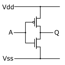
The image on the right shows what happens when an input is connected to both a PMOS transistor (top of diagram) and an NMOS transistor (bottom of diagram). When the voltage of input A is low, the NMOS transistor's channel is in a high resistance state. This limits the current that can flow from Q to ground. The PMOS transistor's channel is in a low resistance state and much more current can flow from the supply to the output. Because the resistance between the supply voltage and Q is low, the voltage drop between the supply voltage and Q due to a current drawn from Q is small. The output, therefore, registers a high voltage.
On the other hand, when the voltage of input A is high, the PMOS transistor is in an OFF (high resistance) state so it would limit the current flowing from the positive supply to the output, while the NMOS transistor is in an ON (low resistance) state, allowing the output from drain to ground. Because the resistance between Q and ground is low, the voltage drop due to a current drawn into Q placing Q above ground is small. This low drop results in the output registering a low voltage.
In short, the outputs of the PMOS and NMOS transistors are complementary such that when the input is low, the output is high, and when the input is high, the output is low. Because of this behavior of input and output, the CMOS circuit's output is the inverse of the input.
The power supplies for CMOS are called VDD and VSS, or VCC and Ground(GND) depending on the manufacturer. VDD and VSS are carryovers from conventional MOS circuits and stand for the drain and source supplies.[6] These do not apply directly to CMOS, since both supplies are really source supplies. VCC and Ground are carryovers from TTL logic and that nomenclature has been retained with the introduction of the 54C/74C line of CMOS.
Duality
An important characteristic of a CMOS circuit is the duality that exists between its PMOS transistors and NMOS transistors. A CMOS circuit is created to allow a path always to exist from the output to either the power source or ground. To accomplish this, the set of all paths to the voltage source must be the complement of the set of all paths to ground. This can be easily accomplished by defining one in terms of the NOT of the other. Due to the De Morgan's laws based logic, the PMOS transistors in parallel have corresponding NMOS transistors in series while the PMOS transistors in series have corresponding NMOS transistors in parallel.
Logic

More complex logic functions such as those involving AND and OR gates require manipulating the paths between gates to represent the logic. When a path consists of two transistors in series, both transistors must have low resistance to the corresponding supply voltage, modelling an AND. When a path consists of two transistors in parallel, either one or both of the transistors must have low resistance to connect the supply voltage to the output, modelling an OR.
Shown on the right is a circuit diagram of a NAND gate in CMOS logic. If both of the A and B inputs are high, then both the NMOS transistors (bottom half of the diagram) will conduct, neither of the PMOS transistors (top half) will conduct, and a conductive path will be established between the output and Vss (ground), bringing the output low. If both of the A and B inputs are low, then neither of the NMOS transistors will conduct, while both of the PMOS transistors will conduct, establishing a conductive path between the output and Vdd (voltage source), bringing the output high. If either of the A or B inputs is low, one of the NMOS transistors will not conduct, one of the PMOS transistors will, and a conductive path will be established between the output and Vdd (voltage source), bringing the output high. As the only configuration of the two inputs that results in a low output is when both are high, this circuit implements a NAND (NOT AND) logic gate.
An advantage of CMOS over NMOS logic is that both low-to-high and high-to-low output transitions are fast since the (PMOS) pull-up transistors have low resistance when switched on, unlike the load resistors in NMOS logic. In addition, the output signal swings the full voltage between the low and high rails. This strong, more nearly symmetric response also makes CMOS more resistant to noise.
See Logical effort for a method of calculating delay in a CMOS circuit.
Example: NAND gate in physical layout
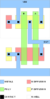
This example shows a NAND logic device drawn as a physical representation as it would be manufactured. The physical layout perspective is a "bird's eye view" of a stack of layers. The circuit is constructed on a P-type substrate. The polysilicon, diffusion, and n-well are referred to as "base layers" and are actually inserted into trenches of the P-type substrate. (See steps 1 to 6 in the process diagram below right) The contacts penetrate an insulating layer between the base layers and the first layer of metal (metal1) making a connection.
The inputs to the NAND (illustrated in green color) are in polysilicon. The CMOS transistors (devices) are formed by the intersection of the polysilicon and diffusion; N diffusion for the N device & P diffusion for the P device (illustrated in salmon and yellow coloring respectively). The output ("out") is connected together in metal (illustrated in cyan coloring). Connections between metal and polysilicon or diffusion are made through contacts (illustrated as black squares). The physical layout example matches the NAND logic circuit given in the previous example.
The N device is manufactured on a P-type substrate while the P device is manufactured in an N-type well (n-well). A P-type substrate "tap" is connected to VSS and an N-type n-well tap is connected to VDD to prevent latchup.
Power: switching and leakage
CMOS logic dissipates less power than NMOS logic circuits because CMOS dissipates power only when switching ("dynamic power"). On a typical ASIC in a modern 90 nanometer process, switching the output might take 120 picoseconds, and happens once every ten nanoseconds. NMOS logic dissipates power whenever the transistor is on, because there is a current path from Vdd to Vss through the load resistor and the n-type network.
Static CMOS gates are very power efficient because they dissipate nearly zero power when idle. Earlier, the power consumption of CMOS devices was not the major concern while designing chips. Factors like speed and area dominated the design parameters. As the CMOS technology moved below sub-micron levels the power consumption per unit area of the chip has risen tremendously.
Broadly classifying, power dissipation in CMOS circuits occurs because of two components, static and dynamic:
Static dissipation
Both NMOS and PMOS transistors have a gate–source threshold voltage, below which the current (called sub threshold current) through the device drops exponentially. Historically, CMOS designs operated at supply voltages much larger than their threshold voltages (Vdd might have been 5 V, and Vth for both NMOS and PMOS might have been 700 mV). A special type of the CMOS transistor with near zero threshold voltage is the native transistor.
SiO2 is a good insulator, but at very small thickness levels electrons can tunnel across the very thin insulation; the probability drops off exponentially with oxide thickness. Tunnelling current becomes very important for transistors below 130 nm technology with gate oxides of 20 Å or thinner.
Small reverse leakage currents are formed due to formation of reverse bias between diffusion regions and wells (for e.g., p-type diffusion vs. n-well), wells and substrate (for e.g., n-well vs. p-substrate). In modern process diode leakage is very small compared to sub threshold and tunnelling currents, so these may be neglected during power calculations.
If the ratios do not match, then there might be different currents of PMOS and NMOS; this may lead to imbalance and thus improper current causes the CMOS to heat up and dissipate power unnecessarily.
Dynamic dissipation
Charging and discharging of load capacitances
CMOS circuits dissipate power by charging the various load capacitances (mostly gate and wire capacitance, but also drain and some source capacitances) whenever they are switched. In one complete cycle of CMOS logic, current flows from VDD to the load capacitance to charge it and then flows from the charged load capacitance (CL) to ground during discharge. Therefore, in one complete charge/discharge cycle, a total of Q=CLVDD is thus transferred from VDD to ground. Multiply by the switching frequency on the load capacitances to get the current used, and multiply by the average voltage again to get the characteristic switching power dissipated by a CMOS device: .

Since most gates do not operate/switch at every clock cycle, they are often accompanied by a factor , called the activity factor. Now, the dynamic power dissipation may be re-written as .


A clock in a system has an activity factor α=1, since it rises and falls every cycle. Most data has an activity factor of 0.1.[7] If correct load capacitance is estimated on a node together with its activity factor, the dynamic power dissipation at that node can be calculated effectively.
Short-circuit power dissipation
Since there is a finite rise/fall time for both pMOS and nMOS, during transition, for example, from off to on, both the transistors will be on for a small period of time in which current will find a path directly from VDD to ground, hence creating a short-circuit current. Short-circuit power dissipation increases with rise and fall time of the transistors.
An additional form of power consumption became significant in the 1990s as wires on chip became narrower and the long wires became more resistive. CMOS gates at the end of those resistive wires see slow input transitions. During the middle of these transitions, both the NMOS and PMOS logic networks are partially conductive, and current flows directly from VDD to VSS. The power thus used is called crowbar power. Careful design which avoids weakly driven long skinny wires ameliorates this effect, but crowbar power can be a substantial part of dynamic CMOS power.
To speed up designs, manufacturers have switched to constructions that have lower voltage thresholds but because of this a modern NMOS transistor with a Vth of 200 mV has a significant subthreshold leakage current. Designs (e.g. desktop processors) which include vast numbers of circuits which are not actively switching still consume power because of this leakage current. Leakage power is a significant portion of the total power consumed by such designs. Multi-threshold CMOS (MTCMOS), now available from foundries, is one approach to managing leakage power. With MTCMOS, high Vth transistors are used when switching speed is not critical, while low Vth transistors are used in speed sensitive paths. Further technology advances that use even thinner gate dielectrics have an additional leakage component because of current tunnelling through the extremely thin gate dielectric. Using high-κ dielectrics instead of silicon dioxide that is the conventional gate dielectric allows similar device performance, but with a thicker gate insulator, thus avoiding this current. Leakage power reduction using new material and system designs is critical to sustaining scaling of CMOS.[8]
Analog CMOS
Besides digital applications, CMOS technology is also used in analog applications. For example, there are CMOS operational amplifier ICs available in the market. Transmission gates may be used as analog multiplexers instead of signal relays. CMOS technology is also widely used for RF circuits all the way to microwave frequencies, in mixed-signal (analog+digital) applications.
Temperature range
Conventional CMOS devices work over a range of –55 °C to +125 °C.
There were theoretical indications as early as August 2008 that silicon CMOS will work down to –233 °C (40 K).[9] Functioning temperatures near 40 K have since been achieved using overclocked AMD Phenom II processors with a combination of liquid nitrogen and liquid helium cooling.[10]
Single-electron CMOS transistors
Ultra small (L = 20 nm, W = 20 nm) CMOS transistors achieve the single-electron limit when operated at cryogenic temperature over a range of –269 °C (4 K) to about –258 °C (15 K). The transistor displays Coulomb blockade due to progressive charging of electrons one by one. The number of electrons confined in the channel is driven by the gate voltage, starting from an occupation of zero electrons, and it can be set to one or many.[11]
See also
- Active pixel sensor
- Beyond CMOS
- Electric (software) – used to lay out CMOS circuits
- FEOL (front-end-of-line) – the first part of IC fabrication process
- Gate equivalent – a technology-independent measure of circuit complexity
- HCMOS – high-speed CMOS 1982
- Magic (software) – used to lay out CMOS circuits
- MOSFET
- CMOS Amplifiers
References
- ↑ COS-MOS was an RCA trademark, which forced other manufacturers to find another name – CMOS
- ↑ "What is CMOS Memory?". Wicked Sago. Archived from the original on 26 September 2014. Retrieved 3 March 2013.
- ↑ Fairchild. Application Note 77. "CMOS, the Ideal Logic Family" Archived 2015-01-09 at the Wayback Machine.. 1983.
- ↑ "Intel® Architecture Leads the Microarchitecture Innovation Field". Intel. Archived from the original on 29 June 2011. Retrieved 2 May 2018.
- ↑ Baker, R. Jacob (2008). CMOS: circuit design, layout, and simulation (Second ed.). Wiley-IEEE. p. xxix. ISBN 978-0-470-22941-5.
- ↑ "Archived copy" (PDF). Archived (PDF) from the original on 2011-12-09. Retrieved 2011-11-25.
- ↑ K. Moiseev, A. Kolodny and S. Wimer, "Timing-aware power-optimal ordering of signals", ACM Transactions on Design Automation of Electronic Systems, Volume 13 Issue 4, September 2008, ACM
- ↑ A good overview of leakage and reduction methods are explained in the book Leakage in Nanometer CMOS Technologies Archived 2011-12-02 at the Wayback Machine. ISBN 0-387-25737-3.
- ↑ Edwards C, "Temperature control", Engineering & Technology 26 July – 8 August 2008, IET
- ↑ Patrick Moorhead (January 15, 2009). "Breaking Records with Dragons and Helium in the Las Vegas Desert". blogs.amd.com/patmoorhead. Archived from the original on September 15, 2010. Retrieved 2009-09-18.
- ↑ Prati, E.; De Michielis, M.; Belli, M.; Cocco, S.; Fanciulli, M.; Kotekar-Patil, D.; Ruoff, M.; Kern, D. P.; Wharam, D. A.; Verduijn, J.; Tettamanzi, G. C.; Rogge, S.; Roche, B.; Wacquez, R.; Jehl, X.; Vinet, M.; Sanquer, M. (2012). "Few electron limit of n-type metal oxide semiconductor single electron transistors" (PDF). Nanotechnology. 23 (21): 215204. arXiv:1203.4811. Bibcode:2012Nanot..23u5204P. doi:10.1088/0957-4484/23/21/215204. PMID 22552118. Archived (PDF) from the original on 2014-10-04.
Further reading
- Baker, R. Jacob (2010). CMOS: Circuit Design, Layout, and Simulation, Third Edition. Wiley-IEEE. p. 1174. ISBN 978-0-470-88132-3. http://CMOSedu.com
- Weste, Neil H. E.; Harris, David M. (2010). CMOS VLSI Design: A Circuits and Systems Perspective, Fourth Edition. Boston: Pearson/Addison-Wesley. p. 840. ISBN 978-0-321-54774-3. http://CMOSVLSI.com/
- Veendrick, H. J. M. (2017). Nanometer CMOS ICs, from Basics to ASICs. Springer. p. 770. ISBN 978-3-319-47595-0. http://springer.com/cn/book/9783319475950?referer=springer.com
- Mead, Carver A. and Conway, Lynn (1980). Introduction to VLSI systems. Boston: Addison-Wesley. ISBN 0-201-04358-0.
- Savard, John J. G. (2018) [2005]. "What Computers Are Made From". quadibloc. Archived from the original on 2018-07-02. Retrieved 2018-07-16.
External links
| Wikimedia Commons has media related to CMOS. |
- CMOS gate description and interactive illustrations
- LASI is a "general purpose" IC layout CAD tool. It is a free download and can be used as a layout tool for CMOS circuits.