MOS Technology 6502
The MOS Technology 6502 (typically "sixty-five-oh-two" or "six-five-oh-two")[3] is an 8-bit microprocessor that was designed by a small team led by Chuck Peddle for MOS Technology. The design team had formerly worked at Motorola on the Motorola 6800 project; the 6502 is essentially a simplified, less expensive and faster version of that design.
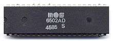 A MOS Technology 6502 processor in a DIP-40 plastic package. The four-digit date code indicates it was made in the 45th week (November) of 1985. | |
| General Info | |
|---|---|
| Launched | 1975 |
| Common manufacturer(s) |
|
| Performance | |
| Max. CPU clock rate | 1 MHz to 3 MHz |
| Data width | 8 |
| Address width | 16 |
| Architecture and classification | |
| Instruction set | MOS 6502 |
| Instructions | 56 |
| Physical specifications | |
| Transistors | |
| Package(s) |
|
| History | |
When it was introduced in 1975, the 6502 was, by a considerable margin, the least expensive microprocessor on the market. It initially sold for less than one-sixth the cost of competing designs from larger companies, such as the 6800 or Intel 8080. Its introduction caused rapid decreases in pricing across the entire processor market. Along with the Zilog Z80, it sparked a series of projects that resulted in the home computer revolution of the early 1980s.
Popular home video game consoles and computers, such as the Atari 2600, Atari 8-bit family, Apple II, Nintendo Entertainment System, Commodore 64, Atari Lynx, BBC Micro and others, used the 6502 or variations of the basic design. Soon after the 6502's introduction, MOS Technology was purchased outright by Commodore International, who continued to sell the microprocessor and licenses to other manufacturers. In the early days of the 6502, it was second-sourced by Rockwell and Synertek, and later licensed to other companies.
In its CMOS form, the 65C02, which was developed by the Western Design Center (WDC), the 6502 family continues to be widely used in embedded systems, with estimated production volumes in the hundreds of millions.[4]
History and use
Origins at Motorola

The 6502 was designed by many of the same engineers that had designed the Motorola 6800 microprocessor family.[5] Motorola started the 6800 microprocessor project in 1971 with Tom Bennett as the main architect. The chip layout began in late 1972, the first 6800 chips were fabricated in February 1974 and the full family was officially released in November 1974.[6][7] John Buchanan was the designer of the 6800 chip[8][9] and Rod Orgill, who later did the 6501, assisted Buchanan with circuit analyses and chip layout.[10] Bill Mensch joined Motorola in June 1971 after graduating from the University of Arizona (at age 26).[11] His first assignment was helping define the peripheral ICs for the 6800 family and later he was the principal designer of the 6820 Peripheral Interface Adapter (PIA).[12] Motorola's engineers could run analog and digital simulations on an IBM 370-165 mainframe computer.[13] Bennett hired Chuck Peddle in 1973 to do architectural support work on the 6800 family products already in progress.[14] He contributed in many areas, including the design of the 6850 ACIA (serial interface).[15]
Motorola's target customers were established electronics companies such as Hewlett-Packard, Tektronix, TRW, and Chrysler.[16] In May 1972, Motorola's engineers began visiting select customers and sharing the details of their proposed 8-bit microprocessor system with ROM, RAM, parallel and serial interfaces.[17] In early 1974, they provided engineering samples of the chips so that customers could prototype their designs. Motorola's "total product family" strategy did not focus on the price of the microprocessor, but on reducing the customer's total design cost. They offered development software on a timeshare computer, the "EXORciser" debugging system, onsite training and field application engineer support.[18][19] Both Intel and Motorola had initially announced a $360 price for a single microprocessor.[20][21] The actual price for production quantities was much less. Motorola offered a design kit containing the 6800 with six support chips for $300.[22]
Peddle, who would accompany the salespeople on customer visits, found that customers were put off by the high cost of the microprocessor chips.[23] At the same time, these visits invariably resulted in the engineers he presented to producing lists of required instructions that were much smaller than "all these fancy instructions" that had been included in the 6800.[24] Peddle and other team members started outlining the design of an improved feature, reduced size microprocessor. At that time, Motorola's new semiconductor fabrication facility in Austin, Texas, was having difficulty producing MOS chips, and mid-1974 was the beginning of a year-long recession in the semiconductor industry. Also, many of the Mesa, Arizona, employees were displeased with the upcoming relocation to Austin.[25]
Motorola's Semiconductor Products Division management was overwhelmed with problems and showed no interest in Peddle's low-cost microprocessor proposal. Eventually Peddle was given an official letter telling him to stop working on the system.[26] Peddle responded to the order by informing Motorola that the letter represented an official declaration of "project abandonment", and as such, the intellectual property he had developed to that point was now his.[27] In a November 1975 interview, Motorola's Chairman, Robert Galvin, ultimately agreed that Peddle's concept was a good one and that the division missed an opportunity, "We did not choose the right leaders in the Semiconductor Products division." The division was reorganized and the management replaced. The new group vice-president John Welty said, "The semiconductor sales organization lost its sensitivity to customer needs and couldn't make speedy decisions."[28]
Moving to MOS Technology

Peddle began looking outside Motorola for a source of funding for this new project. He initially approached MOSTEK CEO L. J. Sevin, but Sevin declined and later admitted this was because he was afraid Motorola would sue them.[29]
While Peddle was visiting Ford Motor Company on one of his sales trips, Bob Johnson, later head of Ford's engine automation division, mentioned that their former colleague John Paivinen had moved to General Instrument and taught himself semiconductor design. He had since moved on and was doing some very interesting work on calculator chipsets at a new company he formed in Valley Forge, Pennsylvania.[30]
Paivinen had formed MOS Technology in 1969 with two other executives from General Instrument, Mort Jaffe and Don McLaughlin. Allen-Bradley, a supplier of electronic components and industrial controls, acquired a majority interest in 1970.[31] The company designed and fabricated custom ICs for customers and had developed a line of calculator chips.[32]
After the MOSTEK efforts fell through, Peddle approached Paivinen, who "immediately got it".[33] On 19 August 1974, Chuck Peddle, Bill Mensch, Rod Orgill, Harry Bawcom, Ray Hirt, Terry Holdt, and Wil Mathys left Motorola to join MOS. Mike Janes joined later. Of the seventeen chip designers and layout people on the 6800 team, seven left. The goal of the team was to design and produce a low-cost microprocessor for embedded applications and to target as wide as possible a customer base. This would be possible only if the microprocessor was low cost, and the price goal was set at $5 in volume.[34]
The original 6800 chips were intended to be 180 × 180 mils,[lower-alpha 1] but layout was completed at 212 × 212 mils (5.4 × 5.4 mm), or an area of 29.0 mm2.[35] For the new design, the cost goal demanded a size goal of 153 × 168 mils (3.9 × 4.3 mm), or an area of 16.6 mm2.[36] Several new techniques would be needed to hit this goal.
Moving to NMOS
Chips are produced by printing multiple copies of the chip design on the surface of a "wafer", a thin disk of highly pure silicon. Smaller chips can be printed in greater numbers on the same wafer, decreasing their relative price. Additionally, wafers always include some number of tiny physical defects that are scattered across the surface of the disk. Any chip printed in that location will fail and has to be discarded. Smaller chips mean any one is less likely to be printed on a defect. For both of these reasons, the cost of the final product is strongly dependant on the size of the chip design.[37] There were two significant advances that arrived in the market just as the 6502 was being designed that provided significant cost reductions.
The first was the move from PMOS to NMOS. PMOS circuits always had power running through them, even in the "off" state. To make changes from on to off easily visible in the signals, most PMOS systems used two positive voltages, often +12 V and +5 V, as well as ground and a negative voltage. An example is the Intel 8080, which had +12 V, +5 V, −5 V and ground.[38] In contrast, NMOS circuits, also known as "depletion-load" transistors, used about half as much energy and thus could be built smaller, reducing the chip size. They also required only a single feed voltage, typically +5 V, which simplified wiring on the chip and further reduced size.[39]
A further practical advantage was that the clock signal for PMOS CPUs had to be strong enough to survive all the dissipation as it traveled through the circuits, which almost always required a separate external chip that could supply a strong enough signal. With the reduced power requirements of NMOS, the clock could be moved onto the chip, simplifying the overall computer design. These changes greatly reduced complexity and the cost of implementing a complete system.[39]
Another change that was taking place was the introduction of contact-less projections systems by Perkin-Elmers in 1973. Previously, chips were patterned onto the surface of the wafer by placing a "mask" on the surface and then shining a bright light on it. The masks were fragile and lasted only a few dozen applications before wearing out. The Micralign system instead projected the image from a distance, so the masks lasted much longer. This did not reduce the size of the resulting designs, but meant that the production line could be run much more efficiently, lowering costs.[40]
MOS Technology's existing fabrication lines were based on the older PMOS technology, they had not yet begun to work with NMOS when the team arrived. Paivinen promised to have an NMOS line up and running in time to begin the production of the new CPU. He delivered on the promise, the new line was ready by June 1975.[41]
Design notes
Chuck Peddle, Rod Orgill, and Wil Mathys designed the initial architecture of the new processors. A September 1975 article in EDN magazine gives this summary of the design:[42]
The MOS Technology 650X family represents a conscious attempt of eight former Motorola employees who worked on the development of the 6800 system to put out a part that would replace and outperform the 6800, yet undersell it. With the benefit of hindsight gained on the 6800 project, the MOS Technology team headed by Chuck Peddle, made the following architectural changes in the Motorola CPU…
The main change in terms of chip size was the elimination of the three-state bus. This had been included in the 6800 to allow it to work with other chips in direct memory access (DMA) and co-processing roles, at the cost of significant die space. In practice, using such a system required the other devices to be similarly complex, and designers instead tended to use off-chip systems to coordinate such access. The 6502 simply removed this feature, in keeping with its design as an inexpensive controller being used for specific tasks and communicating with simple devices. Peddle suggested that anyone that actually required this style of access could implement it with a single 74158.[36]
The next major difference was to simplify the registers. To start with, one of the two accumulators was removed. General-purpose registers like accumulators have to be accessed by many parts of the instruction decoder, and thus require significant amounts of wiring to move data to and from their storage. Two accumulators makes many coding tasks easier, but costs the chip design itself significant complexity.[42] Further savings were made by reducing the stack register from 16 to 8 bits, meaning that the stack could only be 256 bytes long, which was enough for its intended role as a microcontroller.[42]
The 16-bit IX index register was split in two, becoming X and Y. More importantly, the style of access changed; in the 6800, IX held a 16-bit address, which was offset by a number supplied with the instruction, the two were added to produce the final address. In the 6502 (and most other designs), the base address was stored in the instruction, and the X or Y was added to it.[43]
Finally, the instruction set was simplified, freeing up room in the decoder and control logic. Of the original 72 instructions in the 6800, 56 were left. Among those removed were any instruction that moved data between the 6800's two accumulators, as well as a number of branch instructions inspired by the PDP-11 like the ability to directly compare two numeric values. The 6502 used a simpler system that handled comparisons by performing math on the accumulator and then examining result flags.[43]
The chip's high-level design had to be turned into drawings of transistors and interconnects. At MOS Technology, the "layout" was a very manual process done with color pencils and vellum paper. The layout consisted of thousands of polygon shapes on six different drawings; one for each layer of the fabrication process. Given the size limits, the entire chip design had to be constantly considered. Mench and Paivinen worked on the instruction decoder[44] while Mench, Peddle and Orgill worked on the ALU and registers. A further advance, developed at a party, was a way to share some of the internal wiring to allow the ALU to be reduced in size.[45]
In spite of their best efforts, the final design ended up being 5 mils too wide.[46] The first 6502 chips were 168 × 183 mils (4.3 × 4.7 mm), or an area of 19.8 mm2. The rotate right instruction (ROR) did not work in the first silicon, so the instruction was temporarily omitted from the published documents, but the next iteration of the design shrank the chip and corrected the rotate right instruction, which was then included in revised documentation.[47]
Introducing the 6501 and 6502
MOS would introduce two microprocessors based on the same underlying design: the 6501 would plug into the same socket as the Motorola 6800, while the 6502 re-arranged the pinout to support an on-chip clock oscillator. Both would work with other support chips designed for the 6800. They would not run 6800 software because they had a different instruction set, different registers, and mostly different addressing modes.[48] Rod Orgill was responsible for the 6501 design; he had assisted John Buchanan at Motorola on the 6800. Bill Mensch did the 6502; he was the designer of the 6820 Peripheral Interface Adapter (PIA) at Motorola. Harry Bawcom, Mike Janes and Sydney-Anne Holt helped with the layout.
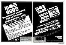
MOS Technology's microprocessor introduction was quite different from the traditional months-long product launch. The first run of a new integrated circuit is normally used for internal testing and shared with select customers as "engineering samples". These chips often have a minor design defect or two that will be corrected before production begins. Chuck Peddle's goal was to sell the first run 6501 and 6502 chips to the attendees at the Wescon trade show in San Francisco beginning on September 16, 1975. Peddle was a very effective spokesman and the MOS Technology microprocessors were extensively covered in the trade press. One of the earliest was a full-page story on the MCS6501 and MCS6502 microprocessors in the July 24, 1975 issue of Electronics magazine.[49] Stories also ran in EE Times (August 24, 1975),[50] EDN (September 20, 1975), Electronic News (November 3, 1975), Byte (November 1975)[51] and Microcomputer Digest (November 1975).[52] Advertisements for the 6501 appeared in several publications the first week of August 1975. The 6501 would be for sale at Wescon for $20 each.[53] In September 1975, the advertisements included both the 6501 and the 6502 microprocessors. The 6502 would cost only $25.[54]
When MOS Technology arrived at Wescon, they found that exhibitors were not permitted to sell anything on the show floor. They rented the MacArthur Suite at the St. Francis Hotel and directed customers there to purchase the processors. At the suite, the processors were stored in large jars to imply that the chips were in production and readily available. The customers did not know the bottom half of each jar contained non-functional chips.[55] The chips were $20 and $25 while the documentation package was an additional $10. Users were encouraged to make photocopies of the documents, an inexpensive way for MOS Technology to distribute product information. The processors were supposed to have 56 instructions, but the Rotate Right (ROR) instruction did not work correctly on these chips, so the preliminary data sheets listed just 55 instructions. The reviews in Byte and EDN noted the lack of the ROR instruction. The next revision of the layout fixed this problem and the May 1976 datasheet listed 56 instructions. Peddle wanted every interested engineer and hobbyist to have access to the chips and documentation; other semiconductor companies only wanted to deal with "serious" customers. For example, Signetics was introducing the 2650 microprocessor and its advertisements asked readers to write for information on their company letterhead.[56]

| Pin | 6800 | 6501 | 6502 |
|---|---|---|---|
| 2 | Halt | Ready | Ready |
| 3 | ∅1 (in) | ∅1 (in) | ∅1 (out) |
| 5 | Valid memory address | Valid memory address | N.C. |
| 7 | Bus available | Bus available | SYNC |
| 36 | Data bus enable | Data bus enable | N.C. |
| 37 | ∅2 (in) | ∅2 (in) | ∅0 (in) |
| 38 | N.C. | N.C. | Set overflow flag |
| 39 | Three-state control | N.C. | ∅2 (out) |
Motorola lawsuit
The 6501/6502 introduction in print and at Wescon was an enormous success. The downside was that the extensive press coverage got Motorola's attention. In October 1975, Motorola reduced the price of a single 6800 microprocessor from $175 to $69. The $300 system design kit was reduced to $150 and it now came with a printed circuit board.[57] On November 3, 1975, Motorola sought an injunction in Federal Court to stop MOS Technology from making and selling microprocessor products. They also filed a lawsuit claiming patent infringement and misappropriation of trade secrets. Motorola claimed that seven former employees joined MOS Technology to create that company's microprocessor products.[58]
Motorola was a billion-dollar company with a plausible case and lawyers. On October 30, 1974, Motorola had filed numerous patent applications on the microprocessor family and was granted twenty-five patents. The first was in June 1976 and the second was to Bill Mensch on July 6, 1976, for the 6820 PIA chip layout. These patents covered the 6800 bus and how the peripheral chips interfaced with the microprocessor.[59] Motorola began making transistors in 1950 and had a portfolio of semiconductor patents. Allen-Bradley decided not to fight this case and sold their interest in MOS Technology back to the founders. Four of the former Motorola engineers were named in the suit: Chuck Peddle, Will Mathys, Bill Mensch and Rod Orgill. All were named inventors in the 6800 patent applications. During the discovery process, Motorola found that one engineer, Mike Janes, had ignored Peddle's instructions and brought his 6800 design documents to MOS Technology.[60] In March 1976, the now independent MOS Technology was running out of money and had to settle the case. They agreed to drop the 6501 processor, pay Motorola $200,000 and return the documents that Motorola contended were confidential. Both companies agreed to cross-license microprocessor patents.[61] That May, Motorola dropped the price of a single 6800 microprocessor to $35. By November, Commodore had acquired MOS Technology.[62][63]
Computers and games
With legal troubles behind them, MOS was still left with the problem of getting developers to try their processor, prompting Chuck Peddle to design the MDT-650 ("microcomputer development terminal") single-board computer. Another group inside the company designed the KIM-1, which was sold semi-complete and could be turned into a usable system with the addition of a 3rd party computer terminal and compact cassette drive. Much to their amazement, the KIM-1 sold well to hobbyists and tinkerers, as well as to the engineers to which it had been targeted. The related Rockwell AIM 65 control/training/development system also did well. The software in the AIM 65 was based on that in the MDT. Another roughly similar product was the Synertek SYM-1.
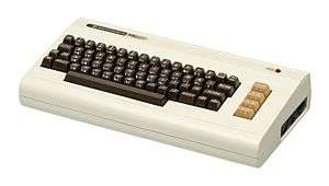
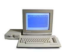
One of the first "public" uses for the design was the Apple I microcomputer, introduced in 1976. The 6502 was next used in the Commodore PET and the Apple II,[64] both released in 1977. It was later used in the Atari 8-bit family and Acorn Atom home computers, the BBC Micro,[64] Commodore VIC-20 and other designs both for home computers and business, such as Ohio Scientific and Oric. The 6510, a direct successor of the 6502 with a digital I/O port and a tri-state address bus, was the CPU utilized in the best-selling[65][66] Commodore 64 home computer. Commodore's floppy disk drive, the 1541, had a processor of its own—it too was a 6502.
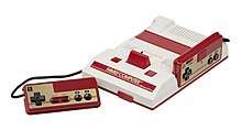
Another important use of the 6500 family was in video games. The first to make use of the processor design was the Atari VCS, later renamed the Atari 2600. The VCS used an offshoot of the 6502 called the 6507, which had fewer pins and, as a result, could address only 8 KB of memory. Millions of the Atari consoles would be sold, each with a MOS processor. Another significant use was by the Nintendo Entertainment System and Famicom. The 6502 used in the NES was a second source version by Ricoh, a partial system-on-a-chip, that lacked the binary-coded decimal mode but added 22 memory-mapped registers and on-die hardware for sound generation, joypad reading, and sprite list DMA. Called 2A03 in NTSC consoles and 2A07 in PAL consoles (the difference being the memory divider ratio and a lookup table for audio sample rates), this processor was produced exclusively for Nintendo. The Atari Lynx used a 4 MHz version of the chip, the 65SC02.
In the 1980s, a popular electronics magazine Elektor/Elektuur used the processor in its microprocessor development board Junior Computer.
- Home computers and video game consoles using the 6502 or its variants
 Apple IIe
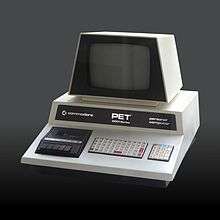 Commodore PET
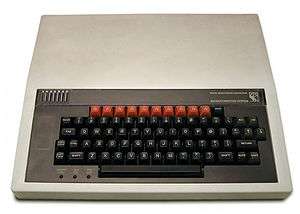
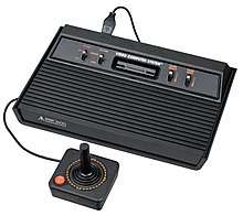 Atari 2600
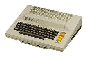
 Ohio Scientific Challenger 4P
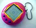 Tamagotchi digital pet[67]
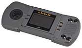 Atari Lynx
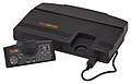 TurboGrafx-16
Technical description

| F | E | D | C | B | A | 9 | 8 | 7 | 6 | 5 | 4 | 3 | 2 | 1 | 0 | (bit position, hex) |
| Main registers | ||||||||||||||||
| A | Accumulator | |||||||||||||||
| Index registers | ||||||||||||||||
| X | X index | |||||||||||||||
| Y | Y index | |||||||||||||||
| 0 | 0 | 0 | 0 | 0 | 0 | 0 | 1 | S | Stack Pointer | |||||||
| Program counter | ||||||||||||||||
| PC | Program Counter | |||||||||||||||
| Status register | ||||||||||||||||
| N | V | - | B | D | I | Z | C | P Processor flags | ||||||||
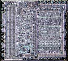
The 6502 is a little-endian 8-bit processor with a 16-bit address bus. The original versions were fabricated using an 8 µm[68] process technology chip with an advertised die size of 153 mils × 168 mils (3.9 mm × 4.3 mm), or an area of 16.6 mm2.[36]
The internal logic runs at the same speed as the external clock rate, but despite the low clock speeds (typically in the neighborhood of 1 to 2 MHz), the 6502's performance was competitive with other contemporary CPUs using significantly faster clocks. This is partly due to a simple state machine implemented by combinational (clockless) logic to a greater extent than in many other designs; the two-phase clock (supplying two synchronizations per cycle) can thereby control the whole machine-cycle directly. Typical instructions might take half as many cycles to complete on the 6502 than contemporary designs. Like most simple CPUs of the era, the dynamic NMOS 6502 chip is not sequenced by a microcode ROM but uses a PLA (which occupied about 15% of the chip area) for instruction decoding and sequencing. As in most 8-bit microprocessors, the chip does some limited overlapping of fetching and execution.
The low clock frequency moderated the speed requirement of memory and peripherals attached to the CPU, as only about 50% of the clock cycle was available for memory access (due to the asynchronous design, this fraction varied strongly among chip versions). This was critical at a time when affordable memory had access times in the range 250–450 ns. The original NMOS 6502 was minimalistically engineered and efficiently manufactured, and therefore cheap—an important factor in getting design wins in the very price-sensitive game-console and home-computer markets.
Registers
Like its precursor, the 6800, the 6502 has very few registers. The 6502's registers include one 8-bit accumulator register (A), two 8-bit index registers (X and Y), 7 processor status flag bits (P), an 8-bit stack pointer (S), and a 16-bit program counter (PC). This compares to a typical design of the same era, the Z80, which has eight general-purpose 8-bit registers, which can be combined into four 16-bit ones. The Z80 also had a complete set of alternate registers which made a total of sixteen general-purpose registers. In order to make up somewhat for the lack of registers, the 6502 included a zero-page addressing mode that uses one address byte in the instruction instead of the two needed to address the full 64 KB of memory. This provides fast access to the first 256 bytes of RAM by using shorter instructions. Chuck Peddle has said in interviews that the specific intention was to allow these first 256 bytes of RAM to be used like registers.
The stack address space is hardwired to memory page $01, i.e. the address range $0100–$01FF (256–511). Software access to the stack is done via four implied addressing mode instructions, whose functions are to push or pop (pull) the accumulator or the processor status register. The same stack is also used for subroutine calls via the JSR (jump to subroutine) and RTS (return from subroutine) instructions and for interrupt handling.
Addressing
The chip uses the index and stack registers effectively with several addressing modes, including a fast "direct page" or "zero page" mode, similar to that found on the PDP-8, that accesses memory locations from addresses 0 to 255 with a single 8-bit address (saving the cycle normally required to fetch the high-order byte of the address)—code for the 6502 uses the zero page much as code for other processors would use registers. On some 6502-based microcomputers with an operating system, the operating system uses most of zero page, leaving only a handful of locations for the user.
Addressing modes also include implied (1-byte instructions); absolute (3 bytes); indexed absolute (3 bytes); indexed zero-page (2 bytes); relative (2 bytes); accumulator (1); indirect,x and indirect,y (2); and immediate (2). Absolute mode is a general-purpose mode. Branch instructions use a signed 8-bit offset relative to the instruction after the branch; the numerical range −128..127 therefore translates to 128 bytes backward and 127 bytes forward from the instruction following the branch (which is 126 bytes backward and 129 bytes forward from the start of the branch instruction). Accumulator mode uses the accumulator as an effective address and does not need any operand data. Immediate mode uses an 8-bit literal operand.
Indirect addressing
The indirect modes are useful for array processing and other looping. With the 5/6 cycle "(indirect),y" mode, the 8-bit Y register is added to a 16-bit base address read from zero page, which is located by a single byte following the opcode. The Y register is therefore an index register in the sense that it is used to hold an actual index (as opposed to the X register in the 6800, where a base address was directly stored and to which an immediate offset could be added). Incrementing the index register to walk the array byte-wise takes only two additional cycles. With the less frequently used "(indirect,x)" mode the effective address for the operation is found at the zero page address formed by adding the second byte of the instruction to the contents of the X register. Using the indexed modes, the zero page effectively acts as a set of up to 128 additional (though very slow) address registers.
The 6502 is capable of performing addition and subtraction in binary or binary-coded decimal. Placing the CPU into BCD mode with the SED (set D flag) instruction results in decimal arithmetic, in which $99 + $01 would result in $00 and the carry (C) flag being set. In binary mode (CLD, clear D flag), the same operation would result in $9A and the carry flag being cleared. Other than Atari BASIC, BCD mode was seldom used in home-computer applications.
See the Hello world! article for a simple but characteristic example of 6502 assembly language.
Instructions and opcodes
6502 instruction operation codes (opcodes) are eight-bits long and have the general form aaabbbcc, where aaa and cc define the opcode, and bbb defines the addressing mode.[69]
For instance, consider the ORA instruction, which performs a bitwise OR on the bits in the accumulator with another value. The instruction opcode is of the form 000bbb01, where bbb may be 010 for an immediate mode value (constant), 001 for zero page fixed address, 011 for an absolute address, and so on.[69]
This pattern is not absolute and there are a number of exceptions. However, where it does apply it allows one to easily deconstruct opcode values back to assembler mnemonics for the majority of instructions, handling the edge cases with special-purpose code.[69]
Of the 256 possible opcodes available using an 8-bit pattern, the original 6502 uses 151 of them, organized into 56 instructions with (possibly) multiple addressing modes. Depending on the instruction and addressing mode, the opcode may require zero, one or two additional bytes for operands. Hence 6502 machine instructions vary in length from one to three bytes.[70][71] The operand is stored in the 6502's customary little-endian format.
The 65C816, the 16-bit CMOS descendant of the 6502, also supports 24-bit addressing, which results in instructions being assembled with three-byte operands, also arranged in little-endian format.
The remaining 105 opcodes are undefined. In the original design, instructions where the low-order 4-bits (nibble) were 3, 7, B or F were not used, providing room for future expansion. Likewise, the $2xxx column had only a single entry, LDX #constant. The remaining 25 empty slots were distributed. Some of the empty slots were used in the 65C02 to provide both new instructions as well as variations on existing ones with new addressing modes. The $Fxxx instructions were initially left free to allow 3rd party vendors to add their own instructions, but later versions of the 65C02 standardized a set of bit fiddling instructions developed by Rockwell Semiconductor.
Assembly language
A 6502 assembly language statement consists of a three-character instruction mnemonic, followed by any operands. Instructions that do not take a separate operand but target a single register based on the addressing mode combine the target register in the instruction mnemonic, so the assembler uses INX as opposed to INC X to increment the X register.
Instruction table
| Opcode matrix for the 6502 instruction set | ||||||||||||
|---|---|---|---|---|---|---|---|---|---|---|---|---|
| Addressing modes: A – accumulator, # – immediate, zpg – zero page, abs – absolute, ind – indirect, X – indexed by X register, Y – indexed by Y register, rel – relative | ||||||||||||
| High nibble | Low nibble | |||||||||||
| 0 | 1 | 2 | 4 | 5 | 6 | 8 | 9 | A | C | D | E | |
| 0 | BRK | ORA (ind,X) | ORA zpg | ASL zpg | PHP | ORA # | ASL A | ORA abs | ASL abs | |||
| 1 | BPL rel | ORA (ind),Y | ORA zpg,X | ASL zpg,X | CLC | ORA abs,Y | ORA abs,X | ASL abs,X | ||||
| 2 | JSR abs | AND (ind,X) | BIT zpg | AND zpg | ROL zpg | PLP | AND # | ROL A | BIT abs | AND abs | ROL abs | |
| 3 | BMI rel | AND (ind),Y | AND zpg,X | ROL zpg,X | SEC | AND abs,Y | AND abs,X | ROL abs,X | ||||
| 4 | RTI | EOR (ind,X) | EOR zpg | LSR zpg | PHA | EOR # | LSR A | JMP abs | EOR abs | LSR abs | ||
| 5 | BVC rel | EOR (ind),Y | EOR zpg,X | LSR zpg,X | CLI | EOR abs,Y | EOR abs,X | LSR abs,X | ||||
| 6 | RTS | ADC (ind,X) | ADC zpg | ROR zpg | PLA | ADC # | ROR A | JMP (ind) | ADC abs | ROR abs | ||
| 7 | BVS rel | ADC (ind),Y | ADC zpg,X | ROR zpg,X | SEI | ADC abs,Y | ADC abs,X | ROR abs,X | ||||
| 8 | STA (ind,X) | STY zpg | STA zpg | STX zpg | DEY | TXA | STY abs | STA abs | STX abs | |||
| 9 | BCC rel | STA (ind),Y | STY zpg,X | STA zpg,X | STX zpg,Y | TYA | STA abs,Y | TXS | STA abs,X | |||
| A | LDY # | LDA (ind,X) | LDX # | LDY zpg | LDA zpg | LDX zpg | TAY | LDA # | TAX | LDY abs | LDA abs | LDX abs |
| B | BCS rel | LDA (ind),Y | LDY zpg,X | LDA zpg,X | LDX zpg,Y | CLV | LDA abs,Y | TSX | LDY abs,X | LDA abs,X | LDX abs,Y | |
| C | CPY # | CMP (ind,X) | CPY zpg | CMP zpg | DEC zpg | INY | CMP # | DEX | CPY abs | CMP abs | DEC abs | |
| D | BNE rel | CMP (ind),Y | CMP zpg,X | DEC zpg,X | CLD | CMP abs,Y | CMP abs,X | DEC abs,X | ||||
| E | CPX # | SBC (ind,X) | CPX zpg | SBC zpg | INC zpg | INX | SBC # | NOP | CPX abs | SBC abs | INC abs | |
| F | BEQ rel | SBC (ind),Y | SBC zpg,X | INC zpg,X | SED | SBC abs,Y | SBC abs,X | INC abs,X | ||||
| Blank opcodes (e.g., F2) and all opcodes whose low nibbles are 3, 7, B and F are undefined in the 6502 instruction set. | ||||||||||||
Detailed behavior
The processor's non-maskable interrupt (NMI) input is edge sensitive, which means that the interrupt is triggered by the falling edge of the signal rather than its level. The implication of this feature is that a wired-OR interrupt circuit is not readily supported. However, this also prevents nested NMI interrupts from occurring until the hardware makes the NMI input inactive again, often under control of the NMI interrupt handler.
The simultaneous assertion of the NMI and IRQ (maskable) hardware interrupt lines causes IRQ to be ignored. However, if the IRQ line remains asserted after the servicing of the NMI, the processor will immediately respond to IRQ, as IRQ is level sensitive. Thus a sort of built-in interrupt priority was established in the 6502 design.
The "Break" flag of the processor is very different from the other flag bits. It has no flag setting, resetting, or testing instructions of its own, and is not affected by the PHP and PLP instructions. It exists only on the stack, where BRK and PHP always write a 1, while IRQ and NMI always write a 0.
The "SO" input pin, when asserted, will set the processor's overflow status bit (deasserting it does not clear the overflow bit, however). This can be used by a high-speed polling device driver, which can poll the hardware once in only three cycles by using a Branch-on-oVerflow-Clear (BVC) instruction that branches to itself. For example, the Commodore 1541 and other Commodore floppy disk drives use this technique to detect without delay whether the serializer is ready to accept or provide another byte of disk data. Obviously great care must be used in the device driver and the associated system design, as spurious assertion of the overflow bit could ruin arithmetic processing.
Variations and derivatives
There were numerous variants of the NMOS 6502:
- The MOS Technology 6503 had reduced memory addressing capability (4 KB) and no RDY input, in a 28-pin DIP package (with the phase 1 (OUT), SYNC, redundant Vss, and SO pins of the 6502 also omitted).[72]
- The MOS Technology 6504 had reduced memory addressing capability (8 KB), no NMI, and no RDY input, in a 28-pin DIP package (with the phase 1 (OUT), SYNC, redundant Vss, and SO pins of the 6502 also omitted).[72]
- The MOS Technology 6505 had reduced memory addressing capability (4 KB) and no NMI, in a 28-pin DIP package (with the phase 1 (OUT), SYNC, redundant Vss, and SO pins of the 6502 also omitted).[72]
- The MOS Technology 6506 had reduced memory addressing capability (4 KB), no NMI, and no RDY input, but all 3 clock pins of the 6502 (i.e. a 2-phase output clock), in a 28-pin DIP package (with the SYNC, redundant Vss, and SO pins of the 6502 also omitted).[72]
- The MOS Technology 6507 had reduced memory addressing capability (8 KB) and no interrupts, in a 28-pin DIP package (with the phase 1 (OUT), SYNC, redundant Vss, and SO pins of the 6502 also omitted).[72] This chip was used in the Atari 2600 video game system.
- The MOS Technology 6508 has a built-in 8-bit input/output port and 256 bytes of internal static RAM.
- The MOS Technology 6509 could address up to 1 MB of RAM as 16 banks of 64 kB and was used in the Commodore CBM-II series.
- The MOS Technology 6510 has a built-in 6-bit programmable input/output port and was used in the Commodore 64.
- The MOS Technology 6512 was a 6502 with a 2-phase clock input for an external clock oscillator, instead of an on-board clock oscillator.[72]
- The MOS Technology 6513 was a 6503 with a 2-phase clock input like the 6512.[72]
- The MOS Technology 6514 was a 6504 with a 2-phase clock input like the 6512.[72]
- The MOS Technology 6515 was a 6505 with a 2-phase clock input like the 6512.[72]
- The Ricoh 2A03 was a 6502 variant including an audio processing unit and lacking the BCD mode, used in the Nintendo Entertainment System.
- The 6502A was a 1.5 MHz chip featured in Asteroids Deluxe.
- The 6502B was a version of the 6502 capable of running at a maximum speed of 2 MHz instead of 1. The B was used in the Apple III, BBC Micro and, clocked at 1.79 MHz, early Atari 8-bit computers
- The “official” 6502C was a version of the original 6502 able to run at up to 4 MHz.
- The Sally, also referred to the 6502C, was a customized 6502 chip used in later Atari 8-bit computers. It has a HALT signal on pin 35 and a second R/W on pin 36 (these pin are not connected (N/C) on a standard 6502s). Pulling HALT low latches the clock, pausing the processor. This was used to sync the CPU with the video circuitry.
- The MOS Technology 6591 and 6592 are System on a chip that utilize a complete Atari 2600 in a 48-pin DIP package.[73][74]
- The 65C02 is a CMOS version of the NMOS 6502 that was designed by Bill Mensch of the Western Design Center, featuring reduced power consumption, support for much higher clock speeds, new instructions, new addressing modes for some existing instructions, and correction of NMOS errata, such as the
JMP ($xxFF)bug. - CSG 65CE02 was a CMOS derivative developed by the Commodore Semiconductor Group (CSG), formerly MOS Technology.
- The Rockwell R65F11 (introduced in 1983) and the later R65F12 are enhanced versions of the 6502-based processor, also including on-chip zero-page RAM, on-chip Forth kernel ROM, a UART, etc.[75][76][77][78]
- The GTE G65SC102 is software compatible with the 65C02, but has a slightly different pinout and oscillator circuit. The BBC Master Turbo included the 4 MHz version of this CPU on a coprocessor card, which could also be bought separately and added to the Master 128.
- The Rockwell R65C00, R65C21, and R65C29 featured two enhanced CMOS 6502s in a single chip, and the R65C00 and R65C21 additionally contained 2 kB of mask-programmable ROM.[79][80]
- The CM630 is an 1 MHz East-bloc clone of the 6502A and was used in the Prawez 8D, a Bulgarian clone of the Oric Atmos.
6512, 6513, 6514, & 6515
The MOS Technology 6512, 6513, 6514, and 6515 each rely on an external clock, instead of using an internal clock generator like the 650x (e.g. 6502). This was used to advantage in some designs where the clocks could be run asymmetrically, increasing overall CPU performance.
The 6512 was used in the BBC Micro B+64.
16-bit derivatives
The Western Design Center designed and currently produces the W65C816S processor, a 16-bit, static-core successor to the 65C02, with greatly enhanced features. The W65C816S is a newer variant of the 65C816, which was the core of the Apple IIGS computer and was the basis of the Ricoh 5A22 processor that powered the popular Super Nintendo Entertainment System. The W65C816S incorporates minor improvements over the 65C816 that make the newer chip not an exact hardware-compatible replacement for the earlier one. Among these improvements was conversion to a static core, which makes it possible to stop the clock in either phase without the registers losing data. Currently available through electronics distributors as of March 2020, the W65C816S is officially rated for 14-megahertz operation.
The Western Design Center also designed and produced the 65C802, which was a 65C816 core with a 64-kilobyte address space in a 65(C)02 pin-compatible package. The 65C802 could be retrofitted to a 6502 board and would function as a 65C02 on power-up, operating in "emulation mode." As with the 65C816, a two-instruction sequence would switch the 65C802 to "native mode" operation, exposing its 16 bit accumulator and index registers, as well as other 65C816 enhanced features. The 65C802 was not widely used; new designs almost always were built around the 65C816, resulting in 65C802 production being discontinued.
Example code
The following 6502 assembly language source code is for a subroutine named TOLOWER, which copies a null-terminated character string from one location to another, converting upper-case letter characters to lower-case letters. The string being copied is the "source", and the string into which the converted source is stored is the "destination".
0080

0080  00 04
0082  00 05

0600

0600  A0 00

0602  B1 80
0604  F0 11

0606  C9 41
0608  90 06

060A  C9 5B
060C  B0 02

060E  09 20

0610  91 82
0612  C8
0613  D0 ED


0615  38
0616  60

0617  91 82
0618  18
0619  60

061A
|
; TOLOWER:
;
;   Convert a null-terminated character string to all lower case.
;   Maximum string length is 255 characters, plus the null term-
;   inator.
;
; Parameters:
;
;   SRC - Source string address
;   DST - Destination string address
;
        ORG $0080
;
SRC     .WORD $0400     ;source string pointer ($40)
DST     .WORD $0500     ;destination string pointer ($42)
;
        ORG $0600       ;execution start address
;
TOLOWER LDY #$00        ;starting index
;
LOOP    LDA (SRC),Y     ;get from source string
        BEQ DONE        ;end of string
;
        CMP #'A'        ;if lower than UC alphabet...
        BCC SKIP        ;copy unchanged
;
        CMP #'Z'+1      ;if greater than UC alphabet...
        BCS SKIP        ;copy unchanged
;
        ORA #%00100000  ;convert to lower case
;
SKIP    STA (DST),Y     ;store to destination string
        INY             ;bump index
        BNE LOOP        ;next character
;
; NOTE: If Y wraps the destination string will be left in an undefined
;  state.  We set carry to indicate this to the calling function.
;
        SEC             ;report string too long error &...
        RTS             ;return to caller
;
DONE    STA (DST),Y     ;terminate destination string
        CLC             ;report conversion completed &...
        RTS             ;return to caller
;
        .END
|
Bugs and quirks
The 6502 had several bugs and quirks, which had to be accounted for when programming it.
- The earliest revisions of the 6502, such as those shipped with some KIM-1 computers, had a severe bug in the ROR (rotate right memory or accumulator) instruction. The operation of ROR in these chips is effectively an ASL (arithmetic shift left) instruction that does not affect the carry bit in the status register. MOS left the instruction out of chip documentation entirely because of the defect, promising that ROR would appear on 6502 chips starting in 1976.[81] The vast majority of 6502 chips in existence today do not exhibit this bug.
- The NMOS 6502 family has a variety of undocumented instructions, which vary from one chip manufacturer to another. The 6502 instruction decoding is implemented in a hardwired logic array (similar to a programmable logic array) that is only defined for 151 of the 256 available opcodes. The remaining 105 trigger strange and occasionally hard-to-predict actions, such as crashing the processor, performing two valid instructions consecutively, performing strange mixtures of two instructions, or simply doing nothing at all. Eastern House Software developed the "Trap65", a device that plugged between the processor and its socket to convert (trap) unimplemented opcodes into BRK (software interrupt) instructions. Some programmers utilized this feature to extend the 6502 instruction set by providing functionality for the unimplemented opcodes with specially written software intercepted at the BRK instruction's 0xFFFE vector.[82][83] All of the undefined opcodes have been replaced with NOP instructions in the 65C02, an enhanced CMOS version of the 6502, although with varying byte sizes and execution times. In the 65C802/65C816, all 256 opcodes perform defined operations.
- The 6502's memory indirect jump instruction,
JMP (<address>), is partly broken. If <address> is hex xxFF (i.e., any word ending in FF), the processor will not jump to the address stored in xxFF andxxFF+1as expected, but rather the one defined by xxFF and xx00 (for example,JMP ($10FF)would jump to the address stored in 10FF and 1000, instead of the one stored in 10FF and 1100). This defect continued through the entire NMOS line, but was corrected in the CMOS derivatives. - The NMOS 6502 indexed addressing across page boundaries will do an extra read of an invalid address. This characteristic may cause random issues by accessing hardware that acts on a read, such as clearing timer or IRQ flags, sending an I/O handshake, etc. This defect continued through the entire NMOS line, but was corrected in the CMOS derivatives, in which the processor does an extra read of the last instruction byte.
- The 6502 read-modify-write instructions perform one read and two write cycles. First, the unmodified data that was read is written back, and then the modified data is written. This characteristic may cause issues by twice accessing hardware that acts on a write. This anomaly continued through the entire NMOS line, but was fixed in the CMOS derivatives, in which the processor will do two reads and one write cycle. Defensive programming practice will generally avoid this problem by not executing read/modify/write instructions on hardware registers.
- The N (result negative), V (sign bit overflow) and Z (result zero) status flags are generally meaningless when performing arithmetic operations while the processor is in BCD mode, as these flags reflect the binary, not BCD, result. This limitation was removed in the CMOS derivatives. Therefore, this feature may be used to distinguish a CMOS processor from an NMOS version.[84]
- If the 6502 happens to be in BCD mode when a hardware interrupt occurs, it will not revert to binary mode. This characteristic could result in obscure bugs in the interrupt service routine if it fails to clear BCD mode before performing any arithmetic operations. For example, the Commodore 64's KERNAL did not correctly handle this processor characteristic, requiring that IRQs be disabled or re-vectored during BCD math operations. This issue was addressed in the CMOS derivatives as well.
- The 6502 instruction set includes BRK (opcode $00), which is technically a software interrupt (similar in spirit to the SWI mnemonic of the Motorola 6800 and ARM processors). BRK is most often used to interrupt program execution and start a machine language monitor for testing and debugging during software development. BRK could also be used to route program execution using a simple jump table (analogous to the manner in which the Intel 8086 and derivatives handle software interrupts by number). Unfortunately, if a hardware interrupt occurs when the processor is fetching a BRK instruction, the NMOS version of the processor will fail to execute BRK and instead proceed as if only a hardware interrupt had occurred. This fault was corrected in the CMOS implementation of the processor.
- When executing JSR (jump to subroutine) and RTS (return from subroutine) instructions, the return address pushed to the stack by JSR is that of the last byte of the JSR operand (that is, the most significant byte of the subroutine address), rather than the address of the following instruction. This is because the actual copy (from program counter to stack and then conversely) takes place before the automatic increment of the program counter that occurs at the end of every instruction.[85] This characteristic would go unnoticed unless the code examined the return address in order to retrieve parameters in the code stream (a 6502 programming idiom documented in the ProDOS 8 Technical Reference Manual). It remains a characteristic of 6502 derivatives to this day.
See also
- List of 6502 assemblers
- MOS Technology 6502-based home computers
- Interrupts in 65xx processors
- Transistor count
- Apple II accelerators
Notes
- At that time the technical literature would state the length and width of each chip in "mils" (0.001 inch).
References
Citations
- "The MOS 6502 and the Best Layout Guy in the World". swtch.com. 2011-01-03. Retrieved 2014-08-09.
- "MOnSter6502". monster6502.com. 2017. Retrieved 2017-05-01.
- William Mensch, Rob Walker (October 9, 1995). Interview with William Mensch (Web video). Atherton, California: Silicon Genesis, Stanford University Libraries. Archived from the original on May 14, 2012. Retrieved June 4, 2012. William Mensch and the moderator both pronounce the 6502 microprocessor as "sixty-five-oh-two".
- "Western Design Center (WDC) Home of 65xx Microprocessor Technology". www.westerndesigncenter.com. Retrieved 2019-04-08.
- "Motorola Sues MOS Technology" (PDF). Microcomputer Digest. Cupertino CA: Microcomputer Associates. 2 (6): 11. December 1975.
- "Motorola joins microprocessor race with 8-bit entry". Electronics. New York: McGraw-Hill. 47 (5): 29–30. March 7, 1974.
- Motorola 6800 Oral History (2008), p. 9
- Buchanan, John K., "MOS DC Voltage booster circuit", US Patent 3942047, issued March 2, 1976.
- Buchanan, John K., "Chip topography for MOS integrated circuitry microprocessor chip", US Patent 3987418, issued October 19, 1976.
- Motorola 6800 Oral History (2008), p. 8
- Mensch Oral History (1995) Mensch earned an Associate degree from Temple University in 1966 and then worked at Philco Ford as an electronics technician before attending the University of Arizona.
- Mensch, William D., "Chip topography for MOS interface circuit", US Patent 3968478, issued July 6, 1976.
- Jenkins, Francis; Lane, E.; Lattin, W.; Richardson, W. (November 1973). "MOS-device modeling for computer implementation". IEEE Transactions on Circuit Theory. IEEE. 20 (6): 649–658. doi:10.1109/tct.1973.1083758. ISSN 0018-9324. All of the authors were with Motorola's Semiconductor Products Division.
- Donohue, James F. (October 27, 1988). "The microprocessor first two decades: The way it was". EDN. Cahners Publishing. 33 (22A): 18–32. ISSN 0012-7515. Page 30. Bennett already was at work on what became the 6800. "He hired me," Peddle says of Bennett, "to do the architectural support work for the product he'd already started." … Peddle says. "Motorola tried to kill it several times. Without Bennett, the 6800 would not have happened, and a lot of the industry would not have happened, either."
- Hepworth, Edward C., Rodney J. Means, Charles I. Peddle, "Asynchronous Communication Interface Adaptor", Patent 3975712, issued August 17, 1976. Note: Motorola typically listed inventors in alphabetical order.
- Motorola (August 5, 1976). "They stay out front with Motorola's M6800 Family". Electronics. McGraw-Hill. 49 (16): 51. Advertisement showing three embedded applications from TRW, HP and RUSCO.
- Motorola 6800 Oral History (2008), p. 89
- "It's the total product family". Electronics. New York: McGraw Hill. 48 (1): 37. January 9, 1975. Motorola advertisement emphasizing their complete set of peripheral chips and development tools. This shorten the customers product design cycle.
- Motorola 6800 Oral History (2008) p. 18
- "Motorola microprocessor set is 1 MHz n-MOS". Control Engineering. 21 (11): 11. November 1974. MC6800 microprocessor price was $360. The MC6850 asynchronous communications interface adaptor (ACIA) was slated for first quarter 1975 introduction.
- Intel Corporation (1984). Kaye, Glynnis Thompson (ed.). A Revolution in Progress - A History to Date of Intel (PDF). Intel Corporation. p. 14. Order number:231295. Archived (PDF) from the original on 23 October 2012. Retrieved 30 December 2016. "Shima implemented the 8080 in about a year and the new device was introduced in April 1974 for $360."
- "Motorola mounts M6800 drive". Electronics. New York: McGraw-Hill. 48 (8): 25. April 17, 1975. "Distributors are being stocked with the M6800 family, and the division is also offering an introductory kit that includes the family's six initial parts, plus applications and programming manuals, for $300."
- Interview 2014, 52:30.
- Interview 2014, 54:45.
- Bagnall (2010), p. 11. Peddle's new offer came at an opportune time for the 6800 developers. "They didn't want to go to Austin, Texas," explains Mensch.
- Interview 2014, 54:40.
- Interview 2014, 55:50.
- Waller, Larry (November 13, 1975). "Motorola seeks to end skid". Electronics. New York: McGraw-Hill. 48 (23): 96–98. Summary: Semiconductor Products split into two parts, integrated circuits and discrete components. Semiconductor losses for the last four quarters exceeded $30 million. The sales organization lost its sensitivity to customer needs, "delays in responding to price cuts meant that customers bought elsewhere." Technical problems plagued IC production. The troubles are "not in design, but in chip and die yields." Problems have been solved. The MC6800 microprocessor "arrived in November 1974."
- Interview 2014, 56:30.
- Interview 2014, 55:00.
- Bagnall (2010), p. 13.
- MOS Technology (November 14, 1974). "The First Single Chip Scientific Calculator Arrays". Electronics. McGraw-Hill. 47 (23): 90–91.
- Interview 2014, 57:00.
- Interview 2014, 58:30.
- Motorola 6800 Oral History (2008), p. 10.
- Cushman 1975, p. 40.
- Ho, Joshua (9 October 2014). "An Introduction to Semiconductor Physics, Technology, and Industry". Anandtech.
- "8080A microprocessor - DIP 40 package". CPU World.
- Cushman 1975, p. 38.
- "Moore's Law Milestones". IEEE.
- Bagnall (2010), p. 19: "Paivinen promised Peddle he would have the n-channel process ready. He was true to his word."
- Cushman 1975, p. 36.
- Cushman 1975, p. 41.
- Interview 2014, 1:01:00.
- Interview 2014, 1:02:00.
- Interview 2014, 1:02:30.
- The August 1975 datasheet had 55 instructions with no ROR, the May 1976 datasheet had the ROR and 56 instructions. File:MCS650x Instruction Set.jpg
- Stanford University, Silicon Genesis project: videotaped oral history interview of Willam Mensch
- "Microprocessor line offers 4, 8,16 bits". Electronics. New York: McGraw-Hill. 48 (15): 118. July 24, 1975. The article covers the 6501 and 6502 plus the 28 pin versions that would only address 4K of memory. It also covered future devices such as "a design that Peddle calls a pseudo 16".
- Sugarman, Robert (25 August 1975). "Does the Country Need A Good $20 Microprocessor?" (PDF). EE Times. Manhasset, New York: CMP Publications: 25. Archived from the original (PDF) on 3 February 2007. Retrieved 5 February 2008.
- Fylstra, Daniel (November 1975). "Son of Motorola (or the $20 CPU Chip)". Byte. Peterborough, NH: Green Publishing. 1 (3): 56–62. Comparison of the 6502 and the 6800 microprocessors. Author visited MOS Technology in August 1975.
- "3rd Generation Microprocessor" (PDF). Microcomputer Digest. Cupertino, CA: Microcomputer Associates. 2 (2): 1–3. August 1975.
- "MOS 6501 Microprocessor beats 'em all". Electronics. New York: McGraw-Hill. 48 (16): 60–61. August 7, 1975.
- "MOS 6502 the second of a low cost high performance microprocessor family". Computer. IEEE Computer Society. 8 (9): 38–39. September 1975. doi:10.1109/C-M.1975.219074.
- Bagnall (2010), pp. 33–35.
- Signetics (October 30, 1975). "Easiest-to-use microprocessor". Electronics. McGraw-Hill. 48 (22): 114–115.
- Motorola (October 30, 1975). "All this and unbundled $69 microprocessor". Electronics. McGraw-Hill. 48 (22): 11. The quantity one price for the MC6800 was reduced from $175 to $69. The previous price for 50 to 99 units was $125.
- Waller, Larry (November 13, 1975). "News briefs: Motorola seeks to stop microprocessor foe". Electronics. New York: McGraw-Hill. 48 (23): 38."Motorola said last week it would seek an immediate injunction to stop MOS Technology Inc., Norristown, Pa., from making and selling microprocessor products, including its MCS6500." (This issue was published on November 7.)
- Motorola was awarded the following US Patents on the 6800 microprocessor family: 3962682, 3968478, 3975712, 3979730, 3979732, 3987418, 4003028, 4004281, 4004283, 4006457, 4010448, 4016546, 4020472, 4030079, 4032896, 4037204, 4040035, 4069510, 4071887, 4086627, 4087855, 4090236, 4145751, 4218740, 4263650.
- Bagnall (2010), p. 53–54. "He [Mike James] had all his original work from the 6800 and hid it from Motorola…
- "Motorola, MOS Technology settle patent suit". Electronics. New York: McGraw-Hill. 49 (7): 39. April 1, 1975. "MOS Technology Inc. of Norristown, Pa. has agreed to withdraw its MCS6501 microprocessor from the market and to pay Motorola Inc. $200000 ..." "MOS Technology and eight former Motorola employees have given back, under court order documents that Motorola contends are confidential." "…both companies have agreed to a cross license relating to patents in the microprocessor field."
- Bagnall (2010), pp. 55-56
- "Mergers and Acquisitions". Mini-Micro Systems. Cahners. 9 (11): 19. November 1976." Commodore International … is buying MOS Technology (Norristown, PA). This saves the six-year-old semiconductor house from impending disaster."
- Goodwins, Rupert (December 4, 2010). "Intel's victims: Eight would-be giant killers". ZDNet. Retrieved March 7, 2012.
- Reimer, Jeremy. "Personal Computer Market Share: 1975-2004". Archived from the original on 6 June 2012. Retrieved 2009-07-17.
- "How many Commodore 64 computers were sold?". Archived from the original on 2016-03-06. Retrieved 2011-02-01.
- "Code Execution on a Tamagotchi". kwartzlab.ca. 7 May 2013. Archived from the original on 2018-08-31. Retrieved 2018-12-23.
- Corder, Mike (Spring 1999). "Big Things in Small Packages". Pioneers' Progress with picoJava Technology. Sun Microelectronics. Archived from the original on 2006-03-12. Retrieved April 23, 2012.
The first 6502 was fabricated with 8 micron technology, ran at one megahertz and had a maximum memory of 64k.
- Parker, Neil. "The 6502/65C02/65C816 Instruction Set Decoded". Neil Parker's Apple II page.
- 6502 Instruction Set.
- NMOS 6502 Opcodes Archived 2016-01-14 at the Wayback Machine.
- 1982 MOS Technology Data Catalog (pdf obtained from bitsavers.org)
- AtariAge: A2600 clone, 6591 chip pinout
- Hackaday: The teensiest Atari 2600 ever
- Randy M. Dumse. "The R65F11 and F68K Single-Chip Forth Computers". Archived 2014-12-02 at the Wayback Machine 1984.
- Ed Schmauch. "A Computerized Corrosion Monitoring System". 1986.
- Lawrence P. Forsley. "Embedded systems: 1990 Rochester Forth Conference : June 12 - 16th, 1990 University of Rochester". p. 51.
- Rockwell. "RSC-Forth User's Manual". 1983.
- "Archived copy" (PDF). Archived from the original (PDF) on 2016-05-15. Retrieved 2014-10-26.CS1 maint: archived copy as title (link)
- "rockwell :: dataBooks :: 1985 Rockwell Data Book" – via Internet Archive.
- "Measuring the ROR Bug in the Early MOS 6502". Retrieved 8 May 2011.
- Moser, Carl W. (January 1979). "Add a Trap Vector for Unimplemented 6502 Opcodes" (PDF). Dr. Dobb's Journal of Computer Calisthenics and Orthodontia. No. 31. Menlo Park, California. p. 32. Retrieved 2017-01-07.
- Harrod, Dennette A. (October 1980). "The 6502 Gets Microprogrammable Instructions". BYTE. Vol. 5 no. 10. Peterborough, New Hampshire. p. 282. Retrieved 2017-01-07.
- Draco (19 June 1997). "65c02, 6502, 65816 ??? CPU sells but who's buying..." Archived from the original on 2 January 2008.
- Andrews, Mark (1984). "6". Atari Roots - A Guide To Atari Assembly Language. ISBN 0-88190-171-7.
Bibliography
- Peddle, Chuck (12 June 2014). "Oral History of Chuck Peddle" (Interview). Interviewed by Doug Fairbairn and Stephen Diamond.
- Bagnall, Brian (2010). Commodore, a company on the edge (2nd ed.). Winnipeg, Manitoba: Variant Press. ISBN 978-0-9738649-6-0.
- Bennett, Thomas; Ekiss, John; Lattin, William (Bill); Lavell, Jeff (28 March 2008). "Motorola 6800 Oral History Panel" (Interview). Interviewed by David Laws. Archived from the original on 2 April 2012.
- Cushman, Robert H. (September 20, 1975). "2-1/2 Generation μP's -$10 Parts That Perform Like Low-End Mini's" (PDF). EDN. Boston: Cahners Publishing. 20 (17): 36–42. Archived from the original (PDF) on 24 April 2016.CS1 maint: ref=harv (link)
- Interview with William Mensch Stanford and the Silicon Valley Project, October 9, 1995. Transcript
Further reading
| Wikibooks has a book on the topic of: 6502 Assembly |
- Datasheets and manuals
- 6500 Series Datasheet; MOS Technology; 12 pages; 1976.
- 6500 Series Hardware Manual; 2nd Ed; MOS Technology; 182 pages; 1976.
- 6500 Series Programming Manual; 2nd Ed; MOS Technology; 262 pages; 1976.
- Books
- 6502 Applications Book; 1st Ed; Rodnay Zaks; Sybex; 281 pages; 1979; ISBN 978-0895880154. (archive)
- 6502 Assembly Language Programming; 2nd Ed; Lance Leventhal; Osborne/McGraw-Hill; 650 pages; 1986; ISBN 978-0078812163. (archive)
- 6502 Assembly Language Subroutines; 1st Ed; Lance Leventhal and Winthrop Saville; Osborne/McGraw-Hill; 550 pages; 1982; ISBN 978-0931988592. (archive)
- 6502 Games; 1st Ed; Rodnay Zaks; Sybex; 292 pages; 1980; ISBN 978-0895880222. (archive)
- 6502 User's Manual; 1st Ed; Joseph Carr; Reston; 288 pages; 1984; ISBN 978-0835970020. (archive)
- Advanced 6502 Programming; 1st Ed; Rodnay Zaks; John Wiley & Sons; 292 pages; 1982; ISBN 978-0895880895. (archive)
- Machine Language For Beginners - Personal Computer Machine Language Programming For Atari, VIC, Apple, C64, and PET Computers; 1st Ed; Richard Mansfield; Compute! Publications; 350 pages; 1983; ISBN 978-0942386110. (archive)
- Programming the 6502; 4th Ed; Rodnay Zaks; Sybex; 408 pages; 1983; ISBN 978-0895881359. (archive)
- Programming the 65816 - including the 6502, 65C02, 65802; 1st Ed; David Eyes and Ron Lichty; Prentice Hall; 636 pages; 1986; ISBN 978-0893037895. (archive)
- Reference cards
- 6502 Microprocessor Instant Reference Card; James Lewis; Micro Logic; 2 pages; 1980. (archive)
%20Microprocessor%20Instant%20Reference%20Card.jpg)
External links
| Wikimedia Commons has media related to 6502 microprocessor. |
- 6502.org - the 6502 microprocessor resource – repository
- The Rise of MOS Technology & The 6502 - Commodore archive
- 650x information – Concise description, photos of MOS and second source chips; at cpu-collection.de
- mdfs.net – 6502 instruction set
- Clever, Eric. "6502 - the first RISC µP". Archived from the original on 24 May 2012.
- Harrod, Dennette A. (October 1980). "6502 Gets Microprogrammable Instructions". BYTE. Vol. 5 no. 10. McGraw Hill. pp. 282–285. ISSN 0360-5280. Archived from the original on 2006-05-25. Retrieved 2006-05-14.
- Simulators / Emulators
- Online 6502 compatible assembler and emulator, written in JavaScript
- List of 6502 software emulators – Zophar's Domain
- 6502 simulator for Windows – Atari Gaming Headquarters
- Visual Transistor-level Simulation of 6502 CPU
- Boards
- Grant's 7/8-chip 6502 board
- 6502 microprocessor training board
- Build your own KIM-1 training board - see KIM-1
- 6502 home computer
- PE6502 single board computer
- FPGA
- cpu6502_tc 6502 CPU core - VHDL source code - OpenCores
- ag_6502 6502 CPU core - Verilog source code - OpenCores
- M65C02 65C02 CPU core - Verilog source code - OpenCores
This article is based on material taken from the Free On-line Dictionary of Computing prior to 1 November 2008 and incorporated under the "relicensing" terms of the GFDL, version 1.3 or later.