Timeline of carbon nanotubes
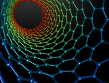 Inside a carbon nanotube | |||||||||||||
|
1952
- Radushkevich and Lukyanovich publish a paper in the Soviet Journal of Physical Chemistry showing hollow graphitic carbon fibers that are 50 nanometers in diameter.[1]
1955
- Hofer, Sterling and McCarney observe a growth of tubular carbon filaments, of 10–200 nm in diameter.[2]
1958
- Hillert and Lange observe a growth of nanoscale tubular carbon filaments from n-heptane decomposition on iron at about 1000 °C.[3]
1960
- Roger Bacon grows "graphite wiskers" in an arc-discharge apparatus and use electron microscopy to show that the structure consist of rolled up graphene sheets in concentric cylinders.[4]
- Bollmann and Spreadborough discuss friction properties of carbon due to rolling sheets of graphene in Nature. Electron Microscope picture clearly shows MWCNT.[5]
1971
- M.L. Lieberman reports growth of three different graphitic like filaments; tubular, twisted, and balloon like.[6] TEM images and diffraction data shows that the hollow tubes are multi-walled carbon nanotubes (MWCNT).
1976
- A. Oberlin, Morinobu Endo, and T. Koyama reported CVD (Chemical Vapor Deposition) growth of nanometer-scale carbon fibers, and they also reported the discovery of carbon nanofibers, including that some were shaped as hollow tubes.[7]
1979
- Arthur C. Clarke's science fiction novel The Fountains of Paradise popularizes the idea of a space elevator using "a continuous pseudo-one dimensional diamond crystal".[8]
1982
- The continuous or floating-catalyst process was patented by Japanese researchers T. Koyama and Morinobu Endo.[9]
1987
- Howard G. Tennent of Hyperion Catalysis issued a U.S. patent for graphitic, hollow core "fibrils".[11]
1991
- Nanotubes synthesized hollow carbon molecules and determined their crystal structure for the first time in the soot of arc discharge at NEC, by Japanese researcher Sumio Iijima.[12]
- August — Nanotubes discovered in CVD by Al Harrington and Tom Maganas of Maganas Industries, leading to development of a method to synthesize monomolecular thin film nanotube coatings.[13]
1992
- First theoretical predictions of the electronic properties of single-walled carbon nanotubes by groups at Naval Research Laboratory, USA;[14] Massachusetts Institute of Technology;[15] and NEC Corporation.[16]
1993
- Groups led by Donald S. Bethune at IBM[17] and Sumio Iijima at NEC[18] independently discover single-wall carbon nanotubes and methods to produce them using transition-metal catalysts.
1995
1997
- First carbon nanotube single-electron transistors (operating at low temperature) are demonstrated by groups at Delft University[21] and UC Berkeley.[22]
- The first suggestion of using carbon nanotubes as optical antennas is made in the patent application of inventor Robert Crowley filed in January 1997.[23]
1998
2000
- First demonstration proving that bending carbon nanotubes changes their resistance[26]
2001
- April — First report on a technique for separating semiconducting and metallic nanotubes.[27]
2002
- January — Multi-walled nanotubes demonstrated to be fastest known oscillators (> 50 GHz).[28]
2003
- September — NEC announced stable fabrication technology of carbon nanotube transistors.[29]
2004
- March — Nature published a photo of an individual 4 cm long single-wall nanotube (SWNT).[30]
2005
- May — A prototype high-definition 10-centimetre flat screen made using nanotubes was exhibited.[31]
- August — University of California finds Y-shaped nanotubes to be ready-made transistors.[32]
- August — General Electric announced the development of an ideal carbon nanotube diode that operates at the "theoretical limit" (the best possible performance). A photovoltaic effect was also observed in the nanotube diode device that could lead to breakthroughs in solar cells, making them more efficient and thus more economically viable.[33]
- August — Nanotube sheet synthesised with dimensions 5 × 100 cm.[34]
2006
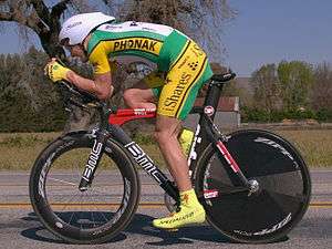
The winning nanotube-enhanced bike ridden by Floyd Landis
- March — IBM announces that they have built an electronic circuit around a CNT.[35]
- March — Nanotubes used as a scaffold for damaged nerve regeneration.[36]
- May — Method of placing nanotube accurately is developed by IBM.[37]
- June — Gadget invented by Rice University that can sort nanotubes by size and electrical properties.[38]
- July — Nanotubes were alloyed into the carbon fiber bike that was ridden by Floyd Landis to win the 2006 Tour de France.[39]
2009
2012
- January — IBM creates 9 nm carbon nanotube transistor that outperforms silicon.[42]
2013
- January – Research team at Rice University announce developing a new wet-spun nanotech fiber.[43] The new fiber is made with an industrial scalable process. The fibers reported in Science have about 10 times the tensile strength and electrical and thermal conductivity of the best previously reported wet-spun CNT fibers.
- September – Researchers build a carbon nanotube computer.[44]
References
- Monthioux, Marc; Kuznetsov, V (2006). "Who should be given the credit for the discovery of carbon nanotubes?" (PDF). Carbon. 44 (9): 1621–1623. doi:10.1016/j.carbon.2006.03.019. Archived from the original on 2006-08-18.CS1 maint: BOT: original-url status unknown (link) ()
- Hofer, L.J.E.; Sterling, E.; McCartney, J.T. (1955). "Structure of the carbon deposited from carbon monoxide on iron, cobalt and nickel". J. Chem. Phys. 59 (11): 1153–1155. doi:10.1021/j150533a010.
- Hillert, M.; Lange, N. (1958). "The Structure of Graphite Filaments". Z. Kristallogr. 111 (1–6): 23–34. Bibcode:1959ZK....111...24H. doi:10.1524/zkri.1959.111.1-6.24.
- Bacon, Roger (1960). "Growth, Structure, and Properties of Graphite Whiskers". J. Appl. Phys. 31 (2): 283. Bibcode:1960JAP....31..283B. doi:10.1063/1.1735559.
- Monthioux, Marc; Spreadborough, J. (1960). "Action of Graphite as Lubricant". Nature. 186 (4718): 29–30. Bibcode:1960Natur.186...29B. doi:10.1038/186029a0.
- Lieberman, M. L.; Hills, C. R.; Miglionico, C. J. (1971). "Growth of graphite filaments". Carbon. 9 (5): 633–635. doi:10.1016/0008-6223(71)90085-6.
- Oberlin, A.; Endo, M.; Koyama, T. (1976). "Filamentous growth of carbon through benzene decomposition". Journal of Crystal Growth. 32 (3): 335–349. Bibcode:1976JCrGr..32..335O. doi:10.1016/0022-0248(76)90115-9.
- "1D Diamond Crystal — A continuous pseudo-one dimensional diamond crystal — maybe a nanotube?". Retrieved 2006-10-21.
"Audacious & Outrageous: Space Elevators". NASA. 7 September 2000. Archived from the original on 19 September 2008. Retrieved 2006-10-21. - Koyama, T. and Endo, M.T. (1983) "Method for Manufacturing Carbon Fibers by a Vapor Phase Process," Japanese Patent 1982-58, 966.
- Kroto, H. W.; et al. (1985). "C60: Buckminsterfullerene". Nature. 318 (6042): 162–163. Bibcode:1985Natur.318..162K. doi:10.1038/318162a0.
- Tennent, Howard G (5 May 1987). "Carbon fibrils, method for producing same and compositions containing same". U.S. Patent 4,663,230. Cite journal requires
|journal=(help) - Iijima, Sumio (7 November 1991). "Helical microtubules of graphitic carbon". Nature. 354 (6348): 56–58. Bibcode:1991Natur.354...56I. doi:10.1038/354056a0.
- Maganas, Thomas C; Alan L. Harrington (1 September 1992). "Intermittent film deposition method and system". U.S. Patent 5,143,745. Cite journal requires
|journal=(help) - Mintmire, J.W.; et al. (3 February 1992). "Are Fullerene Tubules Metallic?". Physical Review Letters. 68 (5): 631–634. Bibcode:1992PhRvL..68..631M. doi:10.1103/PhysRevLett.68.631. PMID 10045950.
- Saito, R.; et al. (15 July 1992). "Electronic structure of graphene tubules based on C60". Physical Review B. 46 (3): 1804–1811. Bibcode:1992PhRvB..46.1804S. doi:10.1103/PhysRevB.46.1804. PMID 10003828.
- Hamada, N.; et al. (9 March 1992). "New One-Dimensional Conductors: Graphitic Microtubules". Physical Review Letters. 68 (10): 1579–1581. Bibcode:1992PhRvL..68.1579H. doi:10.1103/PhysRevLett.68.1579. PMID 10045167.
- Bethune, D. S.; et al. (17 June 1993). "Cobalt-catalysed growth of carbon nanotubes with single-atomic-layer walls". Nature. 363 (6430): 605–607. Bibcode:1993Natur.363..605B. doi:10.1038/363605a0.
- Iijima, Sumio; Toshinari Ichihashi (17 June 1993). "Single-shell carbon nanotubes of 1-nm diameter". Nature. 363 (6430): 603–605. Bibcode:1993Natur.363..603I. doi:10.1038/363603a0.
- de Heer, W. A.; et al. (17 November 1995). "A Carbon Nanotube Field Emission Electron Source". Science. 270 (5239): 1179–1180. Bibcode:1995Sci...270.1179D. doi:10.1126/science.270.5239.1179.
- FIELD-EMISSION CATHODE AND METHOD OF MANUFACTURING IT – Patent EP0801805
- Tans, S.; et al. (3 April 1997). "Individual single-wall carbon nanotubes as quantum wires". Nature. 386 (6624): 474–477. Bibcode:1997Natur.386..474T. doi:10.1038/386474a0.
- Bockrath, M.; et al. (28 March 1997). "Single-Electron Transport in Ropes of Carbon Nanotubes". Science. 275 (5308): 1922–1925. Bibcode:1997APS..MAR.G2504B. doi:10.1126/science.275.5308.1922. PMID 9072967.
- "Patent US6700550 – Optical antenna array for harmonic generation, mixing and signal amplification — Google Patents". Retrieved 2013-01-30.
- Tans, S.; et al. (7 May 1998). "Room-temperature transistor based on a single carbon nanotube". Nature. 393 (6680): 49–52. Bibcode:1998Natur.393...49T. doi:10.1038/29954.
- Martel, R.; et al. (26 October 1998). "Single- and multi-wall carbon nanotube field-effect transistors". Applied Physics Letters. 73 (17): 2447–2449. Bibcode:1998ApPhL..73.2447M. doi:10.1063/1.122477.
- Tombler, Tw; Zhou, C; Alexseyev, L; Kong, J; Dai, H; Liu, L; Jayanthi, Cs; Tang, M; Wu, Sy (Jun 2000). "Reversible electromechanical characteristics of carbon nanotubes under local-probe manipulation". Nature. 405 (6788): 769–72. Bibcode:2000Natur.405..769T. doi:10.1038/35015519. PMID 10866192.
- Collins, Philip; Michael S. Arnold; Phaedon Avouris (27 April 2001). "Engineering Carbon Nanotubes and Nanotube Circuits Using Electrical Breakdown". Science. 292 (5517): 706–709. Bibcode:2001Sci...292..706C. CiteSeerX 10.1.1.474.7203. doi:10.1126/science.1058782. PMID 11326094.
- Minkel, J. R. (18 January 2002). "Nanotubes in the Fast Lane". Physics. 9. doi:10.1103/physrevfocus.9.4. Retrieved 2006-10-21.
- "Tests Verify Carbon Nanotube Enable Ultra High Performance Transistor" (Press release). NEC. 19 September 2003. Retrieved 2006-10-21.
- Zheng, L. X.; et al. (2004). "Ultralong single-wall carbon nanotubes". Nature Materials. 3 (10): 673–676. Bibcode:2004NatMa...3..673Z. doi:10.1038/nmat1216. PMID 15359345.
- "Carbon nanotubes used in computer and TV screens". New Scientist. 21 May 2005. p. 28. Archived from the original on 22 November 2006.
- Knight, Will (15 August 2005). "Y-shaped nanotubes are ready-made transistors". New Scientist Tech. Retrieved 2006-10-21.
- "GE's Research Program Achieves Major Feat in Nanotechnology" (Press release). GE. Archived from the original on 2006-10-15. Retrieved 2006-10-22.
- "Carbon-nanotube fabric measures up". Nanotechweb.org. 18 August 2005.
- "IBM takes step towards chip nanotechnology". CNN Money. 24 March 2006.
Hutson, Stu (23 March 2006). "Nanotube circuit could boost chip speeds".
"Nano circuit offers big promise". BBC News. 24 March 2006. - Marks, Paul (13 March 2006). "Optic nerve regrown with a nanofibre scaffold". New Scientist.
- Kleiner, Kurt (30 May 2006). "Carbon nanotubes pinned down at last". New Scientist.
- Simonite, Tom (27 June 2006). "Gadget sorts nanotubes by size". New Scientist.
- "Carbon nanotubes enter Tour de France". 7 July 2006. Archived from the original on 13 July 2012.
- "New virus-built battery could power cars, electronic devices". 2 April 2009.
- Anne Goodsell; Trygve Ristroph; J. A. Golovchenko; Lene Vestergaard Hau (31 March 2010). "Field Ionization of Cold Atoms near the Wall of a Single Carbon Nanotube". Phys. Rev. Lett. 104 (13): 133002. arXiv:1004.2644. Bibcode:2010PhRvL.104m3002G. doi:10.1103/physrevlett.104.133002. PMC 3113630. PMID 20481881.
- Anthony, Sebastian (26 January 2012). "IBM creates 9nm carbon nanotube transistor that outperforms silicon". ExtremeTech.
- "New nanotech fiber: Robust handling, shocking performance". Rice University News & Media. 10 January 2013.
- "Researchers Build a Working Carbon Nanotube Computer". NY Times. 26 September 2013. Retrieved 26 September 2013.
External links
This article is issued from Wikipedia. The text is licensed under Creative Commons - Attribution - Sharealike. Additional terms may apply for the media files.