Selected area diffraction
Selected area (electron) diffraction (abbreviated as SAD or SAED), is a crystallographic experimental technique that can be performed inside a transmission electron microscope (TEM).
In TEM, a thin crystalline sample is subjected to a parallel beam of high-energy electrons. As TEM samples are typically ~100 nm thick, and the electrons typically have an energy of 100–400 kiloelectron volts, the electrons pass through the sample easily. In this case, electrons are treated as waves, rather than particles (see wave–particle duality). Because the wavelength of high-energy electrons is a few thousandths of a nanometer,[1] and the spacing between atoms in a solid is about a hundred times larger, the electrons are diffracted, and the atoms act as a diffraction grating. Thus, a fraction of the electrons will be scattered to particular angles determined by the crystal structure of the sample, while others pass through the sample without deflection.
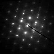
The resulting TEM image will be a series of spots, constituting the selected area diffraction pattern (SADP). Each spot corresponds to a satisfied diffraction condition of the sample's crystal structure. If the sample is tilted, different diffraction conditions will be satisfied, and different diffraction spots will appear.
SAD is referred to as "selected" because the user can easily choose the area of the sample to obtain the diffraction pattern. Located below the sample holder on the TEM column is a selected area aperture, which can be inserted into the beam path. This is a thin strip of metal that will block the beam. It contains several different sized holes, and can be moved by the user. The effect is to block all of the electron beam except for the small fraction passing through one of the holes; by moving the aperture hole to the section of the sample the user wishes to examine, this particular area is selected by the aperture, and only this section will contribute to the SADP on the screen. This is important, for example, in polycrystalline specimens. If more than one crystal contributes to the SADP, it can be difficult or impossible to analyze. As such, it is useful to select a single crystal for analysis at a time. It may also be useful to select two crystals at a time, in order to examine the crystallographic orientation between them.
As a diffraction technique, SAD can be used to identify crystal structures and examine crystal defects. It is similar to X-ray diffraction, but unique in that areas as small as several hundred nanometers in size can be examined, whereas X-ray diffraction typically samples areas several centimeters in size.
A diffraction pattern is made under broad, parallel electron illumination. An aperture in the image plane is used to select the diffracted region of the specimen, giving site-selective diffraction analysis. SAD patterns are a projection of the reciprocal lattice, with lattice reflections showing as sharp diffraction spots. By tilting a crystalline sample to low-index zone axes, SAD patterns can be used to identify crystal structures and measure lattice parameters. SAD is essential for setting up dark-field imaging conditions. Other uses of SAD include analysis of: lattice matching; interfaces; twinning and certain crystalline defects.[2]
SAD is used primarily in material science and solid state physics, and is one of the most commonly used experimental techniques in those fields.
Polycrystalline materials
Single spots appear only when the beam is diffracted by a single crystal. In many materials there are many crystals with different orientations. This is the case for typically made metals as well as powders. SAD of polycrystalline materials gives ring patterns analogous to those from X-ray powder diffraction,[3] and can be used to identify texture and discriminate nanocrystalline from amorphous phases.[2]
References
- David Muller Introduction to Electron Microscopy. p. 13
- SAD Archived 2010-01-11 at the Wayback Machine. CIME. Retrieved on 2011-11-22.
- Williams, David; Carter, C. (2009). Transmission Electron Microscopy: A Textbook For Materials Science. New York, USA: Springer. p. 35. ISBN 978-0-387-76500-6.