OmniVision Technologies
OmniVision Technologies Inc. is a Chinese-owned corporation that designs and develops advanced digital imaging technologies and products for use in mobile phones, notebooks, netbooks and webcams, security and surveillance cameras, entertainment, automotive and medical imaging systems. Headquartered in Santa Clara, California, OmniVision Technologies has offices in the US, Western Europe and Asia, including 5 design centers globally and a testing facility in Shanghai, China.[2]
| Private | |
| Industry | Semiconductors |
| Founded | 1990 |
| Founder | Aucera Technology (Taiwan) |
| Headquarters | , U.S. |
Area served | Worldwide |
Key people | LIN SHYUE JENQ |
| Products | Image sensor technologies |
| Revenue | $1.379B |
| Owner | Will Semiconductor |
Number of employees | 2200 (2015) [1] |
| Website | www.ovt.com |
In 2016, OmniVision was acquired by a consortium of Chinese investors consisting of Hua Capital Management Co., Ltd., CITIC Capital Holdings Limited and Goldstone Investment Co., Ltd.[3]
History
OmniVision was founded in 1995 by Aucera Technology (TAIWAN:奧斯來科技).
Some company milestones:
- 1999: First application-specific IC (ASIC)
- 2000: IPO
- 2002: First mobile handset camera accessory
- 2002: First CMOS image sensor
- 2004: First 1.3-megapixel and 2-megapixel sensors for mobile phones
- 2005: Acquired CDM-Optics, a company founded to commercialize wavefront coding.[4]
- 2006: Introduced the world’s smallest NTS camera
- 2007: Launched first automotive HDR-SOC sensor
- 2008: Launched OmniBSI architecture
- 2009: Introduces first CMOS image sensor for security cameras[5]
- 2010: Acquires Aurora Systems and adds LCOS to its product line[6]
- 2011: Acquired Kodak patents [7]
- 2013: Launched PureCel CMOS image sensors
- 2014: Introduces compact global shutter camera[8]
- 2015: Signed an agreement to be acquired by a group of Chinese investors, including Hua Capital Management, CITIC Capital Holdings and GoldStone Investment, for about $1.9 billion in cash in April 2015.[9]
- 2016: Becomes a private company due to buyout by Chinese private equity consortium[10]
- 2017: Introduces first CMOS image sensor to implement Nyxel™ near-infrared technology[11]
- 2018/2019: Will Semiconductor acquired OmniVision Technologies (for $2.178 billion) and SuperPix Micro Technology, merging them to form Omnivision Group[12][13]
- 2019: Achieved Guinness World Record for world's smallest commercially available sensor for OV6948[14]
- 2019: Launched Nyxel 2 Technology[15]
- 2019: Ships 10 billionth sensor
- 2020: Introduces the world's first automotive grade wafer-level camera[16]
Technologies
OmniPixel3-HS
OmniVision’s front-side illumination (FSI) technology architecture enhances image capture under very low lighting conditions. It is used to manufacture compact cameras in mobile handsets, notebook computers and other applications that require low-light performance without the need for flash.
OmniPixel3-HS is the technology behind its image sensor module that will, for example, be used by Dahua to produce cloud-based cameras for smart home systems.[17]
OmniPixel3-GS expands on its predecessor, and uses global shutter technology to simultaneously expose all pixels and read them out line-by-line for steady, high-speed imaging. Sensitivity to near-infrared (NIR) light means it can capture images that cannot be seen with the human eye. It is used for eye-tracking for facial authentication[18], and other computer vision applications.
OmniBSI
Backside illuminated image (BSI) technology differs from FSI architectures in how light is delivered to the photosensitive area of the sensor. In FSI architectures, the light must first pass through transistors, dielectric layers, and metal circuitry. In contrast, OmniBSI technology turns the image sensor upside down and applies color filters and micro lenses to the backside of the pixels, resulting in light collection through the backside of the sensor. This puts the metal and dielectric layers below the sensor array, providing the most direct path for light to travel into the pixel, which optimizes image quality.
OmniBSI-2
The second-generation BSI technology, developed in cooperation with Taiwan Semiconductor Manufacturing Company Limited (TSMC), is built using custom 65 nm design rules and 300mm copper processes. This combination supports improved low-light sensitivity, dark current, and full-well capacity over the first-generation of BSI technology, as well as sharper image quality.
CameraCubeChip
In this camera module, sensor and lens manufacturing processes are combined using semiconductor stacking methodology. Wafer-level optical elements are fabricated in a single step by combining CMOS image sensors, chip scale packaging processes, (CSP) and wafer-level optics (WLO). These fully integrated chip products have camera functionality and are intended to produce thin, compact devices with advanced imaging capability.
RGB-Ir Technology
RGB-iR technology uses a color filter process to improve color fidelity. By committing 25% of its pixel array pattern to infrared (IR) and 75% to RGB, it can simultaneously capture both RGB and IR images. This makes it possible to capture both day and night images with the same sensor. It is used for battery powered home security cameras as well as biometric authentication, such as gesture and facial recognition.[19]
PureCel Technologies
OmniVision developed its PureCel and PureCel Plus mage sensor technology to provide added camera functionality to smartphones and action cameras. The technical goal was to provide smaller camera modules that enable larger optical formats and offer improved image quality, especially in low-light conditions.[20]
Both of these technologies are offered in a stacked die format (PureCel-S and PureCelPlus-S). This stacked die methodology separates the imaging array from the image sensor processing pipeline into a stacked die structure, allowing for additional functionality to be implemented on the sensor while providing for much smaller die sizes compared to non-stacked sensors. Unique to PureCelPlus-S are partial deep trench isolation (B-DTI) structures comprising an interfacial oxide, first deposited HfO, TaO, oxide, Ti-based liner, and a tungsten core. This is OmniVision's first DTI structure, and the first metal filled B-DTI trench since 2013.[21]
PureCel Plus uses buried color filter array (BCFA) to collect light with various incident light angles for tolerance improvements. Deep trench isolation reduces crosstalk by creating isolation walls between pixels inside silicon. In PureCel Plus Gen 2, OmniVision improved deep trench isolation for better pixel isolation and low-light performance. Its target application is smartphone video cameras.[22]
Nyxel
Developed to address the low-light and night-vision performance requirements of advanced machine vision, surveillance, and automotive camera applications, OmniVision’s Nyxel NIR imaging technology combines thick-silicon pixel architectures and careful management of the wafer surface texture to improve quantum efficiency (QE). In addition, extended deep trench isolation helps retain modulation transfer function without affecting the sensor’s dark current, further improving night vision capabilities. Unlike conventional NIR approaches, OmniVision’s Nyxel technology achieves 3x QE improvement for 850 nm sensitivity and a 5x QE improvement for 940 nm sensitivity.[23] Performance improvements include image quality, extended image-detection range and a reduced light-source requirement, leading to overall lower system power consumption.[24]
Nyxel 2
This second generation near-infrared technology improves upon the first generation by increasing the silicon thickness to improve imaging sensitivity. Deep trench isolation was extended to address issues with crosstalk without impacting modulation transfer function. Wafer surface has been refined to improve the extended photon path and increase photon-electron conversion. The sensor achieves 25% improvement in the invisible 940-nm NIR light spectrum and a 17% increase in the barely visible 850-nm NIR wavelength over the first-generation technology.[25]
LED Flicker Mitigation and High Dynamic Range
High dynamic range (HDR) imaging relies on algorithms to combined several image captures into one to create a higher quality image than native capture alone. LED lighting can create a flicker effect with HDR. This is a problem for machine vision systems, such as those used in autonomous vehicles. That is because LEDs are ubiquitous in automotive environments, from headlights to traffic lights, road signs and beyond. While the human eye can adapt to LED flickering, machine vision cannot. To mitigate this effect, OmniVision uses split pixel technology. One large photodiode captures a scene using short exposure time. A small photodiode using long exposure simultaneously captures the LED signal. The two images are then joined together in a final picture. The result is a flicker-free image.[26] Ficosa, supplier of digital rear-view vision systems to Audi, has integrated OmniVision HDR sensors with LED flicker mitigation technology into their systems.[27]
Products
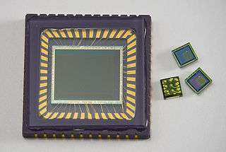
CMOS Image Sensors
OmniVision CMOS image sensors range in resolution from 64 megapixels to below one megapixel.[28]
ASICS
OmniVision also manufactures application integrated circuits (ASICs) as companion products for its image sensors used in automotive, medical, augmented reality and virtual reality (AR/VR), and IoT applications.[29]
CameraCubeChip
OmniVision's CameraCubeChip is a fully packaged, wafer-level camera module measuring 0.65 mm x 0.65 mm that contains the world’s smallest commercially available image sensor. It is being integrated into disposable endoscopes and catheters with diameters as small as 1.0mm. These medical devices are used for a range of medical procedures, from diagnostic to minimally invasive surgery.[30]
LCOS
OmniVision manufacturers liquid crystal on silicon (LCOS) projection technology for display applications.[31]
At CES 2018, together with the Hong Kong Applied Science and Technology Research Institute Company Limited (ASTRI), OmniVision showcased a reference design for a wireless augmented reality headset that could achieve 60 degree field of view (FoV). It combined a single-chip 1080p LCOS display and image sensor from OmniVision with ASTRI's optics and electronics. The headset is said to be smaller and lighter than others because of its single-chip design with integrated driver and memory buffer.[32]
In 2018, AR start-up, Magic Leap, adopted both OmniVision LCOS technology and sensor bridge ASIC for its Magic Leap One mixed reality products.
Markets and Applications
The digital imaging market has converged into two paths: digital photography and machine vision. While smartphone cameras drove the market for some time, since 2017, machine vision applications have driven new developments. Autonomous vehicles, medical devices, miniaturized security cameras, and Internet of Things (IoT) devices all rely on advanced imaging technologies.[33] OmniVision serves every imaging market segment worldwide including:
- Mobile
- Automotive
- Security
- IOT/Emerging
- Computing
- Medical
The following are examples of OmniVision products that have been adopted by end-users.
- The iPhone 5 front-facing camera is an OV2C3B unit.[34]
- In 2014, Google developed 3D mapping technology, Project Tango, for the purpose of bringing AR/VR technology to mobile applications.[35] Tango contains a number of OmniVision products including a 4 MP RGB-Ir sensor that allows for high-res photo and video, as well as depth perception in its standard camera, as well as a low-power CameraChip.[36]
- The Arlo home security camera by Netgear is a battery operated, wireless camera security system. It contains several OmniVision products including the OV00788 as the camera’s image signal processor, and OV9712 a 1.0 megapixel progressive scan CMOS image sensor with video capturing capability.[37]
- The Ring doorbell uses an HD camera that contains a OmniVision OV9712 1MP Image Sensor OmniVision H.264[38] and a video compression chip used for video processing.[39]
- The Sony Playstation contains two OV9713 CMOS image sensors, as well as two USB bridge ASIC solutions. It also appears to have an OV580 ASIC chip that was made specifically for Sony.[40]
- Automotive system supplier ZF included OmniVision CMOS image sensors in its Gen-4 Generation S-Cam in both the mono camera and triple camera set-up.[41]
- As of June 2020, the rear autopilot camera on the Tesla Model S/X/3/Y uses the OV10635 720p CMOS sensor.[42]
- All five models of Asus’ ZenFone 4 smartphone line include dual camera set ups.The mid-range model uses an 8-megapixel OV8856 for both the front camera and the secondary sensor to provides a 120-degree super wide view. The ZenFone 4 Selfie uses a low 5-megapixel resolution OV5670 as its secondary sensor, also for a super-wide view.[43]
- The Microsoft Surface Pro 4 comes with an 8 MP rear camera with the OV5693 image sensor, and a 5 MP front facing camera with the OV8865 image sensor. The rear camera has 1.4 micron pixels, and a F/2 aperture for lower light scenarios. The front camera moves to a wider field of view for use with video conferencing. The quality is a bit grainy. [44]
- Qualcomm’s virtual reality design kit (VRDK) was developed to provide a foundation for consumer electronics manufacturers so they could create VR headsets based on Qualcomm’s Snapdragon VR hardware. To achieve positional tracking, the company designed in on-board cameras backed by the OV9282 global shutter image sensor which can capture 1,280 x 800 images at 120Hz, or 180Hz at 640 x 480. Qualcomm chose it based on claims that low latency makes it a good choice for VR headsets.[45]
Awards and Achievements
The Deloitte Technology Fast 50 List for Silicon Valley:
ACG Silicon Valley GROW! Awards
· 2004 Emerging Growth Award[49]
Fortune
· 2005 Ranked #12 100 Fastest Growing Companies and #1 by revenue growth.[50]
· 2006 Ranked #74 100 Fastest Growing Companies[51]
Electronic Design Magazine
· 2008 Best Image Sensor Technology Award (OmniBSI™ Architecture)[52]
· 2010 Best Image Sensor Technology Award (VGA Sensor)[53]
· 2011 Best Image Sensor Technology Award (CMOS Sensor)
Frost & Sullivan 2018 Manufacturing Leadership Award

Smart Products and Services Leadership (Nyxel project)[55]
3D InCites Awards
- 2018 Device of the Year - OS05A20 Image Sensor[56]
- 2019 Device of the Year for OS02C10
- 2019 Device Manufacturer of the Year[57]
- 2020 Device Manufacturer of the Year [58]
2018 AutoSens Brussels Silver Award for Hardware Innovation[59]

2019 Image Sensor Europe Awards Biggest Breakthrough Technology[60]
Vision Systems Design 2019 Innovators Silver Level Honoree Award for OS02C10 CMOS 1080p HDR image sensor[61]
Nyxel OS02C10 named as one of EDN Hot 100 Products for 2019 in the sensor category.[62]
CTO, Boyd Fowler, is #9 on the 2019 Sensor’s Expo Who’s Who in Sensor Tech top 50 list. His notable development achievements include:
- First digital-pixel CMOS image sensor,
- First scientific linear CMOS image sensor with single-electron RMS read noise
- First multi-megapixel scientific area CMOS image sensor with simultaneous high dynamic range (86dB), fast readout (100 frames/second) and ultra-low read noise (1.2e- RMS) (sCMOS)
- First CMOS image sensor for inter-oral dental X-rays with clipped corners for better patient comfort (US7655918B2)[63]
Henry Yang received the 2019 ASPENCORE World Electronics Achievement Awards for Contributor of the Year[64]
2019 Guinness World Book of World Records with the smallest commercially available image sensors (OV6948)[65]
Locations
Headquartered in Santa Clara, CA, OmniVision has additional offices and manufacturing sites around the world including:
- United States: Louisville, Colorado; lllinois; Farmington Hills, Michigan
- China: Shanghai, Beijing, Shenzhen, Wuhan, Xi’an
- Taiwan: Taipei, Hsinchu
- Korea: Seoul
- Japan: Kyoto, Nagoya,Yokohama
- India: Bangalore
- UK: Hampshire
- Germany: Munich
R&D Locations:
United States: Santa Clara
China: Shanghai
Japan: Kyota, Yokohama
Norway: Oslo
References
- "Corporate Fact Sheet" (PDF). 2014. Retrieved 24 September 2015.
- "OmniVision Locations". Retrieved 13 September 2010.
- "Corporate Releases | News & Events | OmniVision". www.ovt.com. Retrieved 11 January 2020.
- Tomkins, Michael R. (28 March 2005). "OmniVision acquires CDM Optics". The Imaging Resource. Retrieved 25 September 2010.
- "CMOS image sensors, stereoscopic microscopes and more". Nature Photonics. 3 (11): 637–637. November 2009. doi:10.1038/nphoton.2009.209. ISSN 1749-4893.
- Inc, OmniVision Technologies. "OmniVision Technologies, Inc. Completes Acquisition of Aurora Systems, Inc". www.prnewswire.com. Retrieved 24 June 2020.
- Koifman, Vladimir (11 April 2011). "OmniVision Acquires 850 Kodak Patents for $65M". Image Sensor World. Retrieved 15 November 2015.
- "StackPath". www.vision-systems.com. Retrieved 18 June 2020.
- "OmniVision to Be Bought by Chinese Investors in $1.9 Billion Deal". re/code. 1 May 2015. Retrieved 4 May 2015.
- Stahl, George (30 April 2015). "OmniVision Agrees to $1.9 Billion Buyout". Wall Street Journal. ISSN 0099-9660. Retrieved 18 June 2020.
- "StackPath". www.vision-systems.com. Retrieved 18 June 2020.
- Koifman, Vladimir (19 January 2020). "Omnivision Aims to Close the Gap with Sony and Samsung and Lead the Market in 1 Year". Image Sensors World. Retrieved 24 January 2020.
- "OmniVision bought quietly by China's Will Semiconductor | eeNews Analog". www.eenewsanalog.com. Retrieved 24 January 2020.
- "Smallest commercially available image sensor". Guinness World Records. Retrieved 18 June 2020.
- "Gen2 NIR Tech Extends Image Sensors' Night Vision". Sensors Daily. 9 March 2020. Retrieved 18 June 2020.
- "OmniVision Unveils World's First Automotive Wafer-Level Camera Module, Enabling Better Driver Monitoring Systems in More Vehicles". Edge AI and Vision Alliance. 2 June 2020. Retrieved 18 June 2020.
- Lin, Melody. "Dahua Partners with OmniVision to Enable The Cloud-based HD Camera". SM Home. Retrieved 4 April 2016.
- "OmniVision announces global shutter image sensors for facial authentication - asmag.com Rankings". www.asmag.com. Retrieved 19 June 2020.
- "OmniVision Releases First 5MP RGB-IR Image Sensor". www.embedded-computing.com. Retrieved 18 June 2020.
- Triggs, Rob. "Who's Who in the smartphone camera business". Android Authority. Retrieved 4 April 2016.
- Fontaine, Ray. "A Survey of Enabling Technologies in Successful Consumer Digital Imaging Products (Part 3: Pixel Isolation Structures)". TechInsights. Retrieved 4 July 2017.
- "OmniVision Introduces OV02K Image Sensor That is Built on PureCel Plus Pixel Technology". news.thomasnet.com. Retrieved 18 June 2020.
- Carroll, James. "Nyxel near infrared technology from OmniVision offers increased quantum efficiency". Vision Systems Design. Retrieved 9 October 2017.
- Dirjish, Matthew. "Near-Infrared Technology Clears Up Night Vision Apps". Sensors Online. SeQuestex LLC. Retrieved 9 October 2017.
- Roos, Gina (9 March 2020). "OmniVision NIR image sensing achieves new quantum efficiency record". Electronic Products. Retrieved 18 June 2020.
- Yoshida, Junko (12 December 2020). "OmniVision Cuts LED Flicker in HDR". EE Times. Retrieved 18 June 2020.
- "Ficosa first to launch a digital rear-view system". eeNews Automotive. 28 September 2018. Retrieved 23 June 2020.
- "Image Sensors | OmniVision". www.ovt.com. Retrieved 23 June 2020.
- "CameraCubeChip™ | OmniVision". www.ovt.com. Retrieved 23 June 2020.
- "New Miniature Camera Module Emerges for Disposable Medical Endoscopes". mddionline.com. 22 October 2019. Retrieved 23 June 2020.
- "LCOS | OmniVision". www.ovt.com. Retrieved 23 June 2020.
- "This AR Headset Surpasses the Field of View of HoloLens, but You Still Won't Wear It in Public". Next Reality. Retrieved 23 June 2020.
- "Beyond the Smartphone: How Digital Imaging is Becoming Ubiquitous". 3D InCites. 2 May 2018. Retrieved 19 June 2020.
- "iPhone 5 Cameras: Sony and Omnivision Win". iFixit. 23 June 2020. Retrieved 23 June 2020.
- "Project Tango Teardown". iFixit. 16 April 2014. Retrieved 23 June 2020.
- "Prototype of Google's Project Tango Goes Under the Knife". iFixit. 23 June 2020. Retrieved 23 June 2020.
- Unifore. "Disassemble/teardown Netgear Arlo Smart Wireless WiFI cameras security system". www.burglaryalarmsystem.com. Retrieved 23 June 2020.
- "Ring Video Doorbell". benchmarking.ihsmarkit.com. 16 May 2016. Retrieved 23 June 2020.
- "Ring Doorbell - Exploitee.rs". www.exploitee.rs. Retrieved 23 June 2020.
- "PlayStation 4 Camera - PS4 Developer wiki". www.psdevwiki.com. Retrieved 23 June 2020.
- ltd, Research and Markets. "ZF S-Cam 4 - Forward Automotive Mono and Tri Camera for Advanced Driver Assistance Systems". www.researchandmarkets.com. Retrieved 23 June 2020.
- "Undocumented | TeslaTap". Retrieved 23 June 2020.
- "ASUS goes dual-camera crazy for its ZenFone 4 series". Engadget. Retrieved 23 June 2020.
- Howse, Brett. "The Microsoft Surface Pro 4 Review: Raising The Bar". www.anandtech.com. Retrieved 23 June 2020.
- Lang, Ben (29 June 2017). "HTC Vive & Lenovo Standalone Headsets to be Based on Qualcomm Reference Design, Components Detailed". Road to VR. Retrieved 23 June 2020.
- "StubHub, Avigen and PortalPlayer Top Categories in Deloitte's Silicon Valley Technology Fast 50 Ranking of Fastest Growing Companies With Each Exceeding 11,000 Percent Revenue Growth Over Five Years". www.businesswire.com. 26 October 2006. Retrieved 24 June 2020.
- "ISTS Worldwide, TeleNav and Theravance Top Categories in Deloitte's Silicon Valley Technology Fast 50 Rankings with Each Exceeding 12,000 Percent Revenue Growth Over Five Years". www.businesswire.com. 31 October 2007. Retrieved 24 June 2020.
- 2008 Silicon Valley Deloitte Technology Fast 50 Awards
- "GROW! Awards | ACG SV". acgsv.org. Retrieved 24 June 2020.
- "FORTUNE's Fastest Growing Companies 2005". money.cnn.com. Retrieved 24 June 2020.
- "FORTUNE's Fastest Growing Companies 2006: Full list". money.cnn.com. Retrieved 24 June 2020.
- Koifman, Vladimir (15 December 2008). "Omnivision Received EDN's Best Of 2008 Award". Image Sensors World. Retrieved 24 June 2020.
- "StackPath". www.electronicdesign.com. Retrieved 24 June 2020.
- "SV150: Rankings of the top 150 public tech companies in the Bay Area". Silicon Valley. 24 April 2016. Retrieved 24 June 2020.
- "2018 Manufacturing Leadership Awards Winners Announced". Manufacturing Leadership Council. 14 March 2018. Retrieved 24 June 2020.
- "Announcing the Winners of the 2018 3D InCites Awards". 3D InCites. 1 March 2018. Retrieved 24 June 2020.
- "2019 3D InCites Awards Vote". 3D InCites. Retrieved 24 June 2020.
- "And the Winners of the 2020 3D InCites Awards Are…". 3D InCites. 14 February 2020. Retrieved 24 June 2020.
- AutoSens (19 September 2018). "AutoSens Awards Winners crowned for 2018". AutoSens Conference. Retrieved 24 June 2020.
- Koifman, Vladimir (14 March 2019). "Recent Image Sensing Awards". Image Sensors World. Retrieved 24 June 2020.
- "StackPath". www.vision-systems.com. Retrieved 24 June 2020.
- EDN, Staff (17 January 2019). "EDN Hot 100 products of 2018: Sensors". EDN. Retrieved 24 June 2020.
- "Sensors Expo 2019: Who's Who In Sensor Tech". FierceElectronics. Retrieved 24 June 2020.
- Yoshida, Junko (8 November 2019). "EETimes - Movers and Shakers at Global CEO Summit - Page 19 of 20 -". EETimes. Retrieved 24 June 2020.
- "Smallest commercially available image sensor". Guinness World Records. Retrieved 24 June 2020.