Heterojunction
A heterojunction is an interface that occurs between two layers or regions of dissimilar semiconductors. These semiconducting materials have unequal band gaps as opposed to a homojunction. It is often advantageous to engineer the electronic energy bands in many solid-state device applications, including semiconductor lasers, solar cells and transistors. The combination of multiple heterojunctions together in a device is called a heterostructure, although the two terms are commonly used interchangeably. The requirement that each material be a semiconductor with unequal band gaps is somewhat loose, especially on small length scales, where electronic properties depend on spatial properties. A more modern definition of heterojunction is the interface between any two solid-state materials, including crystalline and amorphous structures of metallic, insulating, fast ion conductor and semiconducting materials.
In 2000, the Nobel Prize in physics was awarded jointly to Herbert Kroemer of the University of California, Santa Barbara, California, USA and Zhores I. Alferov of Ioffe Institute, Saint Petersburg, Russia for "developing semiconductor heterostructures used in high-speed-photography and opto-electronics".
Manufacture and applications
Heterojunction manufacturing generally requires the use of molecular beam epitaxy (MBE)[1] or chemical vapor deposition (CVD) technologies in order to precisely control the deposition thickness and create a cleanly lattice-matched abrupt interface. Commonly, there are two steps for manufacturing heterojunction:
- Preparation of Two-dimensional layered materials. The synthesis of 2D monolayers mainly include the top-down strategy and the bottom-up strategy.[2]
- Top-down: Micromechanical Exfoliation. Simple as it seems, this technique is able to yield high-quality 2D crystal flaks, applied to many common-used 2D materials, such as graphene[3], MoS2, WSe2[4] .
- Bottom-up: Chemical vapor deposition (CVD). This method is mainly used to prepare larger films with more stable quality. One of the most popular application is to adopt it for growing MoS2 uses S and MoO3 as precursors [5].
- Heterostructure assembly. Van der Waals heterojunction (vdWH) can be fabricated by staking prepared monolayer. Both top-down and bottom-up approaches can be applied.
- Top-down: Exfoliation and restacking approach.[6] The first layer should be attached onto a substrate. The second layer can be transferred onto a transparent stamp with sacrificial polymer by wet or dry transfer techniques. The stacking of sheets should be precisely conducted under micromanipulators, and then remove the polymer stamp. This is the most widely applied method.
- Bottom-up: Direct CVD growth of heterostructure layers on top of each other. The growing conditions need to be precisely controlled. For example, graphene, h-BN and TMD vdWHs[7] can be prepared this way.
Despite their expense, heterojunctions have found use in a variety of specialized applications where their unique characteristics are critical:
- Solar cells: Heterojunctions are commonly formed through the interface of a crystalline silicon substrate and an amorphous Silicon passivation layer in solar cells. The Heterojunction with Intrinsic Thin-Layer (HIT) solar cell structure was first developed in 1983[8] and commercialised by Sanyo/Panasonic. HIT solar cells now hold the record for the most efficient single-junction silicon solar cell, with a conversion efficiency of 26.7%.[9]
- Lasers: Using heterojunctions in lasers was first proposed[10] in 1963 when Herbert Kroemer, a prominent scientist in this field, suggested that population inversion could be greatly enhanced by heterostructures. By incorporating a smaller direct band gap material like GaAs between two larger band gap layers like AlAs, carriers can be confined so that lasing can occur at room temperature with low threshold currents. It took many years for the material science of heterostructure fabrication to catch up with Kroemer's ideas but now it is the industry standard. It was later discovered that the band gap could be controlled by taking advantage of the quantum size effects in quantum well heterostructures. Furthermore, heterostructures can be used as waveguides to the index step which occurs at the interface, another major advantage to their use in semiconductor lasers. Semiconductor diode lasers used in CD and DVD players and fiber optic transceivers are manufactured using alternating layers of various III-V and II-VI compound semiconductors to form lasing heterostructures.
- Bipolar transistors: When a heterojunction is used as the base-emitter junction of a bipolar junction transistor, extremely high forward gain and low reverse gain result. This translates into very good high frequency operation (values in tens to hundreds of GHz) and low leakage currents. This device is called a heterojunction bipolar transistor (HBT).
- Field effect transistors: Heterojunctions are used in high electron mobility transistors (HEMT) which can operate at significantly higher frequencies (over 500 GHz). The proper doping profile and band alignment gives rise to extremely high electron mobilities by creating a two dimensional electron gas within a dopant free region where very little scattering can occur.
Energy band alignment
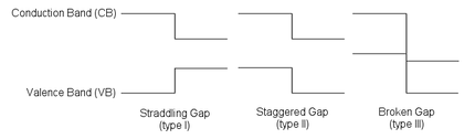
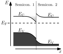
The behaviour of a semiconductor junction depends crucially on the alignment of the energy bands at the interface. Semiconductor interfaces can be organized into three types of heterojunctions: straddling gap (type I), staggered gap (type II) or broken gap (type III) as seen in the figure.[11] Away from the junction, the band bending can be computed based on the usual procedure of solving Poisson's equation.
Various models exist to predict the band alignment.
- The simplest (and least accurate) model is Anderson's rule, which predicts the band alignment based on the properties of vacuum-semiconductor interfaces (in particular the vacuum electron affinity). The main limitation is its neglect of chemical bonding.
- A common anion rule was proposed which guesses that since the valence band is related to anionic states, materials with the same anions should have very small valence band offsets. This however did not explain the data but is related to the trend that two materials with different anions tend to have larger valence band offsets than conduction band offsets.
- Tersoff[12] proposed a gap state model based on more familiar metal-semiconductor junctions where the conduction band offset is given by the difference in Schottky barrier height. This model includes a dipole layer at the interface between the two semiconductors which arises from electron tunneling from the conduction band of one material into the gap of the other (analogous to metal-induced gap states). This model agrees well with systems where both materials are closely lattice matched[13] such as GaAs/AlGaAs.
- The 60:40 rule is a heuristic for the specific case of junctions between the semiconductor GaAs and the alloy semiconductor AlxGa1−xAs. As the x in the AlxGa1−xAs side is varied from 0 to 1, the ratio tends to maintain the value 60/40. For comparison, Anderson's rule predicts for a GaAs/AlAs junction (x=1).[14][15]


The typical method for measuring band offsets is by calculating them from measuring exciton energies in the luminescence spectra.[15]
Effective mass mismatch
When a heterojunction is formed by two different semiconductors, a quantum well can be fabricated due to difference in band structure. In order to calculate the static energy levels within the achieved quantum well, understanding variation or mismatch of the effective mass across the heterojunction becomes substantial. The quantum well defined in the heterojunction can be treated as a finite well potential with width of . Addition to that, in 1966, Conley et al.[16] and BenDaniel and Duke[17] reported boundary condition for the envelope function in quantum well, known as BenDaniel-Duke boundary condition. According to them, the envelope function in fabricated quantum well must satisfy boundary condition which states are both continuous in interface regions.


Using the Schrödinger equation for a finite well with width of and center at 0, the equation for the achieved quantum well can be written as:


Solution for above equations are well-known, only with different(modified) k and [18]

- .

At the z = even-parity solution can be gained from

- .

By taking derivative of (5) and multiplying both sides by

- .

Dividing (6) by (5), even-parity solution function can be obtained,
- .

Similarly, for odd-parity solution,
- .

For numerical solution, taking derivatives of (7) and (8) gives
even parity:

odd parity:

where .

The difference in effective mass between materials results in a larger difference in ground state energies.
Nanoscale heterojunctions
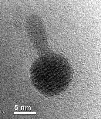
In quantum dots the band energies are dependent on crystal size due to the quantum size effects. This enables band offset engineering in nanoscale heterostructures. It is possible[19] to use the same materials but change the type of junction, say from straddling (type I) to staggered (type II), by changing the size or thickness of the crystals involved. The most common nanoscale heterostructure system is ZnS on CdSe (CdSe@ZnS) which has a straddling gap (type I) offset. In this system the much larger band gap ZnS passivates the surface of the fluorescent CdSe core thereby increasing the quantum efficiency of the luminescence. There is an added bonus of increased thermal stability due to the stronger bonds in the ZnS shell as suggested by its larger band gap. Since CdSe and ZnS both grow in the zincblende crystal phase and are closely lattice matched, core shell growth is preferred. In other systems or under different growth conditions it may be possible to grow anisotropic structures such as the one seen in the image on the right.
It has been shown[20] that the driving force for charge transfer between conduction bands in these structures is the conduction band offset. By decreasing the size of CdSe nanocrystals grown on TiO2, Robel et al.[20] found that electrons transferred faster from the higher CdSe conduction band into TiO2. In CdSe the quantum size effect is much more pronounced in the conduction band due to the smaller effective mass than in the valence band, and this is the case with most semiconductors. Consequently, engineering the conduction band offset is typically much easier with nanoscale heterojunctions. For staggered (type II) offset nanoscale heterojunctions, photoinduced charge separation can occur since there the lowest energy state for holes may be on one side of the junction whereas the lowest energy for electrons is on the opposite side. It has been suggested[20] that anisotropic staggered gap (type II) nanoscale heterojunctions may be used for photocatalysis, specifically for water splitting with solar energy.
See also
- Homojunction, p–n junction—a junction involving two types of the same semiconductor.
- Metal–semiconductor junction—a junction of a metal to a semiconductor.
References
- Smith, C.G (1996). "Low-dimensional quantum devices". Rep. Prog. Phys. 59 (1996) 235282, pg 244.
- Tian, He; Chin, Matthew L.; Najmaei, Sina; Guo, Qiushi; Xia, Fengnian; Wang, Han; Dubey, Madan (2016-04-29). "Optoelectronic devices based on two-dimensional transition metal dichalcogenides". Nano Research. 9 (6): 1543–1560. doi:10.1007/s12274-016-1034-9. ISSN 1998-0124.
- Novoselov, K. S. (2004-10-22). "Electric Field Effect in Atomically Thin Carbon Films". Science. 306 (5696): 666–669. arXiv:cond-mat/0410550. Bibcode:2004Sci...306..666N. doi:10.1126/science.1102896. ISSN 0036-8075.
- Novoselov, K. S.; Jiang, D.; Schedin, F.; Booth, T. J.; Khotkevich, V. V.; Morozov, S. V.; Geim, A. K. (2005-07-18). "Two-dimensional atomic crystals". Proceedings of the National Academy of Sciences. 102 (30): 10451–10453. arXiv:cond-mat/0503533. Bibcode:2005PNAS..10210451N. doi:10.1073/pnas.0502848102. ISSN 0027-8424.
- Zhang, Jing; Yu, Hua; Chen, Wei; Tian, Xuezeng; Liu, Donghua; Cheng, Meng; Xie, Guibai; Yang, Wei; Yang, Rong; Bai, Xuedong; Shi, Dongxia (2014-05-23). "Scalable Growth of High-Quality Polycrystalline MoS2 Monolayers on SiO2 with Tunable Grain Sizes". ACS Nano. 8 (6): 6024–6030. doi:10.1021/nn5020819. ISSN 1936-0851. PMID 24818518.
- Liu, Yuan; Weiss, Nathan O.; Duan, Xidong; Cheng, Hung-Chieh; Huang, Yu; Duan, Xiangfeng (2016-07-12). "Van der Waals heterostructures and devices". Nature Reviews Materials. 1 (9): 16042. Bibcode:2016NatRM...116042L. doi:10.1038/natrevmats.2016.42. ISSN 2058-8437.
- Yan, Aiming; Velasco, Jairo; Kahn, Salman; Watanabe, Kenji; Taniguchi, Takashi; Wang, Feng; Crommie, Michael F.; Zettl, Alex (2015-09-14). "Direct Growth of Single- and Few-Layer MoS2 on h-BN with Preferred Relative Rotation Angles". Nano Letters. 15 (10): 6324–6331. arXiv:1504.06641. Bibcode:2015NanoL..15.6324Y. doi:10.1021/acs.nanolett.5b01311. ISSN 1530-6984.
- Okuda, Koji; Okamoto, Hiroaki; Hamakawa, Yoshihiro (1983). "Amorphous Si/Polycrystalline Si Stacked Solar Cell Having More Than 12% Conversion Efficiency". Japanese Journal of Applied Physics. 22 (9). doi:10.1143/JJAP.22.L605.
- Yamamoto, Kenji; Yoshikawa, Kunta; Uzu, Hisashi; Adachi, Daisuke (2018). "High-efficiency heterojunction crystalline Si solar cells". Japanese Journal of Applied Physics. 57 (8S3). doi:10.7567/JJAP.57.08RB20.
- Kroemer, H. (1963). "A proposed class of hetero-junction injection lasers". Proceedings of the IEEE. 51 (12): 1782–1783. doi:10.1109/PROC.1963.2706.
- Ihn, Thomas (2010). "ch. 5.1 Band engineering". Semiconductor Nanostructures Quantum States and Electronic Transport. United States of America: Oxford University Press. pp. 66. ISBN 9780199534432.
- J. Tersoff (1984). "Theory of semiconductor heterojunctions: The role of quantum dipoles". Physical Review B. 30 (8): 4874–4877. Bibcode:1984PhRvB..30.4874T. doi:10.1103/PhysRevB.30.4874.
- Pallab, Bhattacharya (1997), Semiconductor Optoelectronic Devices, Prentice Hall, ISBN 0-13-495656-7
- Adachi, Sadao (1993-01-01). Properties of Aluminium Gallium Arsenide. ISBN 9780852965580.
- Debbar, N.; Biswas, Dipankar; Bhattacharya, Pallab (1989). "Conduction-band offsets in pseudomorphic InxGa1-xAs/Al0.2Ga0.8As quantum wells (0.07≤x≤0.18) measured by deep-level transient spectroscopy". Physical Review B. 40 (2): 1058. Bibcode:1989PhRvB..40.1058D. doi:10.1103/PhysRevB.40.1058.
- Conley, J.; Duke, C.; Mahan, G.; Tiemann, J. (1966). "Electron Tunneling in Metal-Semiconductor Barriers". Physical Review. 150 (2): 466. Bibcode:1966PhRv..150..466C. doi:10.1103/PhysRev.150.466.
- Bendaniel, D.; Duke, C. (1966). "Space-Charge Effects on Electron Tunneling". Physical Review. 152 (2): 683. Bibcode:1966PhRv..152..683B. doi:10.1103/PhysRev.152.683.
- Griffiths, David J. (2004). Introduction to Quantum Mechanics (2nd ed.). Prentice Hall. ISBN 0-13-111892-7
- Ivanov, Sergei A.; Piryatinski, Andrei; Nanda, Jagjit; Tretiak, Sergei; Zavadil, Kevin R.; Wallace, William O.; Werder, Don; Klimov, Victor I. (2007). "Type-II Core/Shell CdS/ZnSe Nanocrystals: Synthesis, Electronic Structures, and Spectroscopic Properties". Journal of the American Chemical Society. 129 (38): 11708–19. doi:10.1021/ja068351m. PMID 17727285.
- Robel, István; Kuno, Masaru; Kamat, Prashant V. (2007). "Size-Dependent Electron Injection from Excited CdSe Quantum Dots into TiO2Nanoparticles". Journal of the American Chemical Society. 129 (14): 4136–7. doi:10.1021/ja070099a. PMID 17373799.
Further reading
- Bastard, Gérald (1991). Wave Mechanics Applied to Semiconductor Heterostructures. Wiley-Interscience. ISBN 978-0-470-21708-5.
- Feucht, D. Lion; Milnes, A.G. (1970). Heterojunctions and metal-semiconductor junctions. New York City and London: Academic Press., ISBN 0-12-498050-3. A somewhat dated reference respect to applications, but always a good introduction to basic principles of heterojunction devices.
- R. Tsu; F. Zypman (1990). "New insights in the physics of resonant tunneling". Surface Science. 228 (1–3): 418. Bibcode:1990SurSc.228..418T. doi:10.1016/0039-6028(90)90341-5.