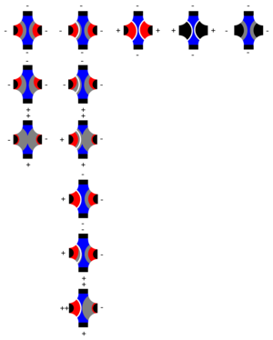
Depletion and enhancement modes
In field-effect transistors (FETS), depletion mode and enhancement mode are two major transistor types, corresponding to whether the transistor is in an ON state or an OFF state at zero gate-source voltage.

Enhancement-mode MOSFETS (metal–oxide–semiconductor FETs) are the common switching elements in most integrated circuits. These devices are off at zero gate–source voltage. NMOS can be turned on by pulling the gate voltage higher than the source voltage, PMOS can be turned on by pulling the gate voltage lower than the source voltage. In most circuits, this means pulling an enhancement-mode MOSFET's gate voltage towards its drain voltage turns it ON.
In a depletion-mode MOSFET, the device is normally ON at zero gate–source voltage. Such devices are used as load "resistors" in logic circuits (in depletion-load NMOS logic, for example). For N-type depletion-load devices, the threshold voltage might be about –3 V, so it could be turned off by pulling the gate 3 V negative (the drain, by comparison, is more positive than the source in NMOS). In PMOS, the polarities are reversed.
The mode can be determined by the sign of the threshold voltage (gate voltage relative to source voltage at the point where an inversion layer just forms in the channel): for an N-type FET, enhancement-mode devices have positive thresholds, and depletion-mode devices have negative thresholds; for a P-type FET, enhancement-mode negative, depletion-mode positive.
Junction field effect - transistors (JFETs) are depletion mode, since the gate junction would forward bias if the gate were taken more than a little from source toward drain voltage. Such devices are used in gallium arsenide and germanium chips, where it is difficult to make an oxide insulator.
Alternative terminology
Some sources say "depletion type" and "enhancement type" for the device types as described in this article as "depletion mode" and "enhancement mode", and apply the "mode" terms for which direction the gate–source voltage differs from zero.[1] Moving the gate voltage toward the drain voltage "enhances" the conduction in the channel, so this defines the enhancement mode of operation, while moving the gate away from the drain depletes the channel, so this defines depletion mode.
Enhancement-load and depletion-load logic families
Depletion-load NMOS logic refers to the logic family that became dominant in silicon VLSI in the latter half of the 1970s; the process supported both enhancement-mode and depletion-mode transistors, and typical logic circuits used enhancement-mode devices as pull-down switches and depletion-mode devices as loads, or pull-ups. Logic families built in older processes that did not support depletion-mode transistors were retrospectively referred to as enhancement-load logic, or as saturated-load logic, since the enhancement-mode transistors were typically connected with gate to the VDD supply and operated in the saturation region (sometimes the gates are biased to a higher VGG voltage and operated in the linear region, for a better power–delay product (PDP), but the loads then take more area).[2] Alternatively, rather than static logic gates, dynamic logic such as four-phase logic was sometimes used in processes that did not have depletion-mode transistors available.
For example, the 1971 Intel 4004 used enhancement-load silicon-gate PMOS logic, and the 1976 Zilog Z80 used depletion-load silicon-gate NMOS.
History
The first MOSFET (metal-oxide-semiconductor field-effect transistor) demonstrated by Egyptian engineer Mohamed M. Atalla and Korean engineer Dawon Kahng at Bell Labs in 1960 was an enhancement mode silicon semiconductor device.[3] In 1963, both depletion and enhancement mode MOSFETs were described by Steve R. Hofstein and Fred P. Heiman at RCA Laboratories.[4] In 1966, T.P. Brody and H.E. Kunig at Westinghouse Electric fabricated enhancement and depletion mode indium arsenide (InAs) MOS thin-film transistors (TFTs).[5][6]
References
- John J. Adams (2001). Mastering Electronics Workbench. McGraw-Hill Professional. p. 192. ISBN 978-0-07-134483-8.
- Jerry C. Whitaker (2005). Microelectronics (2nd ed.). CRC Press. p. 6-7–6-10. ISBN 978-0-8493-3391-0.
- Sah, Chih-Tang (October 1988). "Evolution of the MOS transistor-from conception to VLSI" (PDF). Proceedings of the IEEE. 76 (10): 1280–1326 (1293). doi:10.1109/5.16328. ISSN 0018-9219.
- Hofstein, Steve R.; Heiman, Fred P. (September 1963). "The silicon insulated-gate field-effect transistor". Proceedings of the IEEE. 51 (9): 1190–1202. doi:10.1109/PROC.1963.2488.
- Woodall, Jerry M. (2010). Fundamentals of III-V Semiconductor MOSFETs. Springer Science & Business Media. pp. 2–3. ISBN 9781441915474.
- Brody, T. P.; Kunig, H. E. (October 1966). "A HIGH‐GAIN InAs THIN‐FILM TRANSISTOR". Applied Physics Letters. 9 (7): 259–260. doi:10.1063/1.1754740. ISSN 0003-6951.