Blackmer gain cell
The Blackmer gain cell is an audio frequency voltage-controlled amplifier (VCA) circuit with an exponential control law invented and patented by David E. Blackmer in 1970-1973. Four-transistor core of the original Blackmer cell contains two complementary bipolar current mirrors performing log-antilog operation on input voltages in a push-pull, alternating, fashion. Earlier log-antilog modulators employing the fundamental exponential characteristic of a p–n junction were unipolar; Blackmer's application of push-pull signal processing allowed modulation of bipolar voltages or bidirectional currents.
The Blackmer cell, manufactured since 1973, is historically the first precision VCA circuit suitable for professional audio. As early as in the 1970s production Blackmer cells achieved 110 dB control range with total harmonic distortion of no more than 0.01% and very high compliance with ideal exponential control law. The circuit was used in remote-controlled mixing consoles, signal compressors, microphone amplifiers, and dbx noise reduction systems. In the 21st century, the Blackmer cell remains one of two integrated VCA topologies still widely used in studio and stage equipment, along with Douglas Frey's Operational Voltage Controlled Element (OVCE).[1]
Development and applications
.jpg)
In the 1960-s American recording studios adopted multitrack recording. The number of tracks grew from eight to sixteen, with a proportionate decrease in track width[2]; in the end of 1971 United Recording and Wally Heider put into operation the first 24-track recorders built by MCI.[3] Narrow tracks of multitrack recorders were inevitably noisier than wide tracks of their predecessors; mixing up many narrow tracks further worsened signal-to-noise ratio of master tapes.[2] Mixing became a complex process requiring precisely timed operation of numerous controls and faders - too many of them to operate manually.[2] These problems of early multitrack studios caused demand for professional-grade noise reduction systems and console automation.[2] At the core of both of these functions was the voltage-controlled amplifier.[2]
The earliest solid-state VCA topology, actually an attenuator rather than an amplifier, employed a junction field-effect transistor in voltage-controlled resistance mode.[4] These attenutators, being state of the art in early 1970-s, were successfully used in professional Dolby A and consumer Dolby B noise reduction systems, but could not meet all the demands of professional audio.[4] In 1968 Barry Gilbert invented the Gilbert cell that was quickly adopted by radio and analog computer designers, but again lacked the precision required for studio equipment.[2] Finally, in 1970-1973 David E. Blackmer invented and patented the four-transistor multiplying log-antilog cell, specifically targeting professional audio.[2]1989b
The Blackmer cell surpassed all prior VCA topologies in precision and dynamic range, but it had one important shortcoming. It required well-matched complementary transistors, of both npn and pnp types, that could not yet be implemented in a silicon integrated circuit[2]. Contemporary junction isolation technology offered poor-performing p-n-p transtistors, so integrated cicuit designers had to rely on n-p-n transistors alone[5]. The Gilbert and Dolby circuits were easily integrated in silicon,[6][1] but the Blackmer cell had do be assembled from tediously selected, precision-matched discrete transistors.[2][5] To ensure isothermal operation, these metal-can transistors were firmly held together with a thermally conductive ceramic block and insulated from the environment with a steel can. The first hybrid integrated circuits of this type, the "black can" dbx202, were manufactured by Blackmer's company in 1973. Five years later Blackmer released the improved dbx202C "gold can" hybrid IC; total harmonic distortion decreased from 0.03% to 0.01%, gain control range increased from 110 dB to 116 dB[7]. In 1980 Blackmer released a different version designed by Bob Adams, the dbx2001[8]. Unlike earlier Blackmer cells that operated in lean class AB, the dbx2001 operated in pure class A. Distortion dropped to less than 0.001%, however, noise and dynamic range of dbx2001 were inferior to those of class AB circuits[7]. This, first, generation of Blackmer VCAs had a very long service life; as of 2002, analogue consoles built around the original dbx202 "cans" were still actively used in studios[9].
By 1980 complementary bipolar integrated circuits became a reality, and Allison Research released the first monolithic Blackmer cell IC. The ECG-101, designed by Paul Buff, contained only the core of a modified Blackmer cell - a set of eight matched transistors intended for pure class A operation[10][8]. It had a unique sonic signature, practically devoid of undesirable odd-order harmonics, and was easier to stabilize than the original Blackmer cell[10]. In 1981 dbx, Inc. released their own monolithic IC, the dbx2150/2151/2155 designed by Dave Welland (future co-founder of Silicon Labs)[7][8]. The three numeric designations denoted three different grades of the same chip, 2151 being the best, 2155 the worst; the middle-of-the-line 2150 was by far the most widely used[7]. The 8-pin single-in-line package (SIP8) assured good isolation between inputs and outputs and became the industry standard, used in later ICs like dbx2100, THAT2150 or THAT2181. These circuits, like the original hybrid dbx ICs, always were a small-volume niche product used exclusively in professional analogue audio.[9] Typical applications include mixing consoles, compressors, noise gates, duckers, de-essers and state variable filters[11]. The dbx noise reduction system, which employed the Blackmer cell, had limited success in semi-professional market but failed in consumer markets, losing to Dolby C[12]. The only mass market where dbx managed to get a strong foothold was the North American Multichannel Television Sound, introduced in 1984 and operating until the end of analogue over-the-air television in 2009[13].
In the 21st century professional Blackmer ICs are manufactured by THAT Corporation (a direct descendant of Blackmers' dbx, Inc.) using dielectric isolation technology[5]. As of April 2020, the company offered one dual-channel and two single-channel Blackmer ICs, and four "analog engine" ICs containing Blackmer cells controlled by Blackmer RMS detectors[14].
Operation

Log-antilog principle
The Blackmer cell is a direct descendant of a two-transistor log-antilog circuit, itself a derivative of simple current mirror. Normally, the bases of two transistors of a mirror are tied together, to ensure that collector current I2 of the output transistor T2 exactly mirrors collector current I1 of the input transistor T1. Additional positive or negative bias voltage VY applied between the bases of T1 and T2 converts the mirror into a current amplifier or attenuator[15]. Scale factor, or current gain, follows the exponential Shockley formula:

where it the thermal voltage, proportional to absolute temperature, and equal to 25.852 mV at 300 K[17].

Control voltage VY is usually referenced to ground either with one terminal grounded, or with both terminals driven differentially with precisely zero volts common-mode voltage. This requires lowering emitter potential below ground, usually with an operational amplifier A1 which also converts input voltage VX into input current I1 (so-called transdiode configuration). A second operational amplifier A2 converts output current I2 into output voltage VXY.[18][15]
In mathematics, logarithm function is defined for positive argument only. A log-antilog circuit built with npn transistors will only accept positive input voltage VX, or only negative VX in case of pnp transistors[19][15]. This is unacceptable in audio applications, which have to handle alternating signals.[6] Adding DC offset to audio signal, as was proposed by Embley in 1970[7], will work at a fixed gain setting, but any changes in gain will modulate output DC offset.[6]
Four-transistor Blackmer core
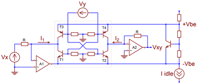
The Blackmer circuit blends two complementary log-antilog VCAs in one.[20] Its four-transistor core (the Blackmer cell proper) combines two complementary current mirrors, wired back-to-back and operating in a push-pull fashion.[21] The lower npn-type mirror (T1, T2) sinks input current I1; the upper pnp-type mirror (T3, T4) is sourcing input current I1 in the opposite direction.[5] A VBE multiplier, thermally coupled to the core, maintains around 1.5 V (2 VBE) across its power supply terminals and regulates its idle current (2 mA or less in production monolithic ICs[14]). Signal voltage is applied to terminals VX, control voltage to terminals VY. Operational amplifiers A1, A2 perform same voltage-to-current and current-to-voltage converter functions as their counterparts in unipolar log-antilog circuit[20], and maintain virtual ground potential at input and output nodes of the core. Values of feedback resistors are usually set at 10 kOhm (100 kOhm in early hybrid ICs)[22]; they must be equal to ensure unity gain at zero control voltage[23]. Potentials of all nodes of the core other than Vy are almost independent of input signals, which is common to all current-mode circuits: they process signal currents, not voltages.
When control voltage VY=0 the core operates as a bidirectional current follower, replicating input current I1 to output current I2. In cores biased to pure class A both mirrors contribute their shares of I2 simultaneously; in cores biased to class AB this is true only for very small values of VX and I1. At higher VX one of the mirrors of a class AB core shuts down, and all output current I2 is sunk or sourced with the other (active) mirror. With positive (negative) VY current through the active mirror (or both mirrors in class A) increases (decreases) exponentially, exactly as it does in a single-quadrant log-antilog circuit:
- assuming equal values of R in A1 and A2[16]


At 300 K, the slope of exponential control law equals 0.33 dB/mV (or 3.0 mV/dB), for either negative of positive values of VX. In practice, the slope is inconveniently steep, and the core is usually decoupled from real-world control voltages with an active attenuator. This attenuator, or any other source of VY, must have very low noise and very low output impedance, attainable only in opamp-based circuits. Single-ended VY drive is almost as good as symmetric balanced drive; having two VY terminals allows control of the cell by two independent single-ended voltages[5].
Gain of the Blackmer cell inversely depends on temperature: the hotter the chip, the lower the slope of exponential control law. For example, VY=+70 mV at 300 K translates to a gain of 10 times, or +20 dB. As the die temperature rises to 310 K, gain at VY=+70 mV decreases by 0.66 dB to +19.3 dB; at maximum operating temperature of 343 K (70 °C) it drops to +17.2 dB. In practice this shortcoming is easily overridden by using control scale that is proportional to absolute temperature (PTAT). In dbx noise reduction system and THAT Corp's "analog engine" this is ensured by the physics of the Blackmer RMS detector, which is PTAT by design. In old mixing consoles the same effect was achieved with PTC (positive temperature coefficient) thermistors[24].
Eight-transistor core
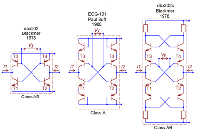
Mismatches of pnp and npn transistors of a basic Blackmer cell are usually balanced with trimming. Alternatively, transistors can be balanced by design, via inclusion of opposite-type diode-wired transistors into each leg of the core. Each of the four legs of the modified core contains one npn and one pnp type transistor; although functionally they are still asymetrical, the degree of asymmetry is greatly reduced. The slope of exponential control law is exactly half of that of the four-transistor cell. This improvement was invented by recording engineer Paul Conrad Buff, and manufactured since 1980 as the monolithic ECG-101 IC by Allison Research and the identical TA-101 by Valley People[25][26].
Eight-transistor core with log error correction
Parasitic base and emitter resistances distort current-voltage characteristics of real-world transistors, introducing logarithming error and distorting output signal. To improve precision beyond what what was attainable through the use of oversized core transistors, Blackmer suggested his own eight-transistor core with interleaved local feedback loops. The circuit, first produced as hybrid dbx202C in 1978, and as monolithic 2150/2151/2155 ICs in 1981, minimizes log-error distortion when the value of each feedback resistor equals the sum of equivalent emitter resistances on npn and pnp-type transistors. A simple model predicts that this approach neutralizes all sources of logarthming error, but in reality feedback cannot compensate for current crowding effects. These can only be reduced by increasing transistor sizes. Cores of monolithic Blackmer ICs are so large that effective feedback resistor values are less than 1 Ohm.[27][25]
Parallel wiring of cores
Blackmer cores, being current-in, current-out devices, can be easily paralleled.[28] Wiring identical cores in parallel increases input and output currents proportionally to the number of cores, however, noise current rises only as the square root of same number. Paralleling four cores, for example, increases signal current four times and increases noise current two times, thus improving signal-to-noise ratio by 6 dB. The first production circuit of this type, the hybrid dbx202x, contained eight parallel cores made up of discrete transistors; the hybrid THAT2002 contained four monolithic THAT2181 dies.[29][30]
Performance
Design of a Blackmer cell IC is always a compromise favouring a specific combination of distortion, noise and dynamic range of gain settings. These properties, critical for professional audio application, are intricately interrelated and cannot be perfected simultaneously. Another compromise that is fixed at die level is the choice of circuit simplicity (built-in, wafer-level trimming) or lowest distortion (external in-circuit trimming)[16][7].
Distortion
Distortion of a class AB Blackmer core has three main sources:
- Logarithming error due to finite parasitic resistances;
- Asymmetry of top (pnp) and bottom (npn) transistors;
- Nonlinearity of input voltage-to-current converter (A1).[20]
The first two sources are contained within the core, and define distortion pattern at low frequencies. Both are suppressed by increasing transistor sizes, although effective neutralization of logarithming error is possible only in improved eight-transistor cores.[31] Larger transistors have lesser parasitic resistances, and are less sensitive to inevitable random area mismatches.[31] Temporal mismatches due to thermal gradients are avoided by careful placement of core transistors and surrounding components on the chip.[32] Residual mismatch of pnp and npn mirrors is compensated with trimming, usually by injection of a very small current into one of two output transistors of the core.[33] This creates a small asymmetric biasing voltage, of the order of a few millivolts or less, which should ideally be proportional to absolute temperature.[33] In monolithic ICs this is ensured by using a thermally-coupled PTAT source of bias current.[33] Wafer-level trimming inevitably suffers from random shifts during subsequent die packaging; wafer-trimmed chips have maximum rated THD from 0.01% (best grade) to 0.05% (worst grade) at 1V RMS input.[34] Further improvements, down to 0.001% THD, require in-circuit fine trimming.[35] It is normally performed once, using a precision THD analyzer, and needs no subsequent adjustments[30].
Output amplifier A2 operates at fixed closed-loop gain, drives a benign constant-impedance load, and does not degrade distortion.[35] Input amplifier A1, on the contrary, drives a nonlinear feedback loop wrapped around the core, and must remain stable at any possible combination of VX and VY.[35] To avoid crossover distortion, A1 must have very high bandwidth and fast slew rate[10], but even then at treble audio frequencies, as open-loop gain of A1 decreases, its nonlinearity becomes the dominant factor of distortion.[35] This type of distortion is common to any operational amplifier with voltage output; in production ICs it is effectively nulled by replacing voltage-output amplifier with a current-output transconductance amplifier.[35][5].
Noise
Estimation and measurement of signal-to-noise ratio is difficult and ambiguous because of complex non-linear relationship between currents, voltages and noise. At zero or very small input signals, the core has a very low noise floor. At higher input signals, this residual noise is swamped by far large modulation noise containing products of shot noise, thermal noise of the core's transistors, and various external noises injected into VY terminals[36]. Higher instant input signals cause greater modulation: "noise follows the signal", in a nonlinear fashion[10].
At moderate gain or attenuation settings noise of the core, assuming noise-free surrounding circuitry, is determined by collector current shot noise which is proportional to square root of emitter current[37]. Thus lowest noise is attained in class AB cores with very small idle currents. Design for lowest distortion, on the contrary, require pure class A operation at the cost of higher noise. For example, in THAT Corp's ICs increase of idle current from 20 μA (class AB) to 750 μA (class A) causes a rise in no-signal noise floor by 17 dB[38]; in dbx, Inc. hybric "cans" the difference was either 10 or 16 dB[7]. In practice, there is no perfect compromise; the choice of low-noise class AB or low-distortion class A depends on application.[39]
Noise of operational amplifiers A1 and A2 is material at very low or very high gain settings. In class AB ICs by THAT Corporation, noise of A2 becomes dominant at gain of −30 dB or less, noise of A2 becomes dominant at gains of +20 dB or more. Finally, at high output levels, noise signature is dominated by noises injected via control terminals, even when proper care has been taken to suppress their sources[36].
Injection of noise and distortion via control terminals
Blackmer cells are particularly sensitive to interference at control terminals. Any signal arriving at VY port, be it useful control voltage or unwanted noise, directly modulates output signal at a rate of 0.33 dB/mV for a four-transistor cell or 0.17 dB/mV for an eight-transistor cell. 1 mV of random noise or hum results in either 4% or 2% modulation, degrading signal-to-noise ratio to absolutely unacceptable 28 dB or 34 dB[40]. Contamination of VY with input signal VX will cause not noise, but unacceptable level of harmonic distortion[30].
Circuits driving VY terminals must be designed as thoroughly as professional-grade audio paths. In practice, VY terminals are usually interfaced to external control signals with low-noise operational amplifiers directly, ensuring lowest possible output impedance[30]; low-cost amplifiers like the NE5532 are an inferior but acceptable alternative to quieter but expensive models.[41] Amplifiers of this class are characterized by audio frequency noise density of a few nV/Hz; although low, it will swamp all other noise sources at high signal levels[42].

Control range
In class AB cores, off-state suppression of input signal, which marks the lowest end of control scale, reaches 110 dB at 1 kHz but deteriorates at higher audio frequencies due to parasitic capacitances. Single-in-line IC packages, otherwise obsolete, perform very good in this respect due to relative long distance between input and output pins. Care should also be taken to prevent capacitive coupling from VX input to A1 non-inverting input[30]. In class A cores, control scale is inevitably narrower due to higher residual noise level[43].
Control voltage feedthrough
In class AB cores, at low frequencies feedthrough of control voltage VY into output signal has two principal sources: mismatches in core transistors, which are reduced by increasing transistor sizes, and feedthrough of input bias current. Any DC component of VX, and input offset voltage of amplifier A1 inject DC components into input current I1, which are replicated at the output and modulated by the core along with AC input signal. These sources of feedthrough can be neutralized with capacitive coupling, leaving just one undesirable DC component, input bias current of A1. This current can be reduced to a few nanoamperes with bias-cancelling input stages. At high frequencies, VY is coupled to the output node directly via collector-base capacitances of the core transistors. Differential VY drive does not eliminate the problem completely due to different capacitances of pnp and npn transistors.[40] Residual VY feedthrough can be nulled by feedforward injection of inverted VY into the output node via a small-value capacitor, restoring capacitive symmetry of the core.[40]
Class A cores, in general, are more prone to control voltage feedthrough owing to thermal gradients in the core (in class AB same gradients manifest themselves as distortion). Early class A ICs used as muting gates produced audible low-frequency "thumps", but subsequent improvements in production ICs significantly reduced the undesirable feedthrough[43].
References
- Tyler & Kirkwood 2008, p. 342.
- Tyler & Kirkwood 2008, p. 341.
- "MCI Unit 'Godsend' at 'Jesus Rock' Sessions". Billboard: 13. 1971-11-06.
- Adams 2006, p. xi.
- Tyler & Kirkwood 2008, p. 344.
- Hebert 1995, p. 2.
- Duncan 1989b, p. 58.
- "A Brief History of VCAs". THAT Corporation. 2019. Retrieved 2020-05-09.
- Israelsohn 2002, p. 41.
- Duncan 1989b, p. 59.
- Tyler & Kirkwood 2008, pp. 344–345.
- Сухов, Н. (1998). "Dolby B, Dolby C, Dolby S ... dbx?". Радиохобби (4): 45–48.CS1 maint: ref=harv (link)
- Jones, Graham (2013). National Association of Broadcasters Engineering Handbook: NAB Engineering Handbook. Taylor & Francis. pp. 1520–1523. ISBN 9781136034107.CS1 maint: ref=harv (link)
- "THAT IC Selection Guide". THAT Corporation. 2019. Retrieved 2020-04-26.
- Duncan 1989a, p. 88.
- Israelsohn 2002, p. 40.
- Sabah, Nassir (2017). Electronics: Basic, Analog, and Digital with PSpice. CRC Press. p. 703. ISBN 9781420087086.
- Hebert 1995, p. 2, Figure 1.
- Tyler & Kirkwood 2008, p. 343.
- Hebert 1995, p. 3.
- Tyler & Kirkwood 2008, pp. 343–344.
- THAT Corporation 2002, p. 2.
- THAT Corporation 2002, p. 4.
- THAT Corporation 2002, p. 7.
- Duncan 1989b, pp. 58, 59.
- Tyler & Kirkwood 2008, p. 341, 344.
- Hebert 1995, p. 5.
- THAT Corporation 2002, p. 3.
- THAT Corporation 2002, pp. 3, 5.
- Self 2010, p. 499.
- Hebert 1995, pp. 6–7.
- Hebert 1995, p. 6.
- Hebert 1995, p. 7.
- Hebert 1995, pp. 7–8.
- Hebert 1995, p. 8.
- Hebert 1995, p. 14.
- Hebert 1995, p. 9.
- Hebert 1995, pp. 10–11.
- Hebert 1995, p. 11.
- Hebert 1995, p. 12.
- THAT Corporation (2010). "Improving VCA Performance II & III" (PDF). THAT Corporation Design Note 110: 2.CS1 maint: ref=harv (link)
- Hebert 1995, pp. 12, 14.
- Duncan 1989b, p. 60.
Bibliography
- Adams, Robert (2006). "Foreword". In Gordon W. Roberts, Vincent W. Leung (ed.). Design and Analysis of Integrator-Based Log-Domain Filter Circuits. Springer Science & Business Media. ISBN 9780306470547.
- Dow, Ron; Parks, Dan (1990). "Understanding and Using VCAs". Broadcast Engineering (September): 84–94.
- Duncan, Ben (1989a). "VCAs Investigated. Part One". Studio Sound (June): 82–88.
- Duncan, Ben (1989b). "VCAs Investigated. Part Two". Studio Sound (July): 58–62.
- Hebert, Gary K. (1995). "An Improved Monolithic Voltage-Controlled Amplifier" (PDF). AES Convention Paper Forum. 99th Convention, 1995 October 6-9: 1–35. (preprint)
- Israelsohn, Joshua (2002). "Gain Control" (PDF). Electronic Design News (August): 38–46.
- Self, Douglas (2010). Small Signal Audio Design. Focal Press / Elsevier. ISBN 9780240521770.
- THAT Corporation (2002). "Upgrading Modular VCAs" (PDF). THAT Corporation Design Note 127: 1–8.
- Tyler, Les; Kirkwood, Wayne (2008). "12.3.4 Dedicated Analog Integrated Circuits for Audio Applications". In Glen Ballou (ed.). Handbook for Sound Engineers. Fourth Edition. Focal/Elsevier. ISBN 978-0-240-80969-4.