Via (electronics)
A via or VIA (Latin for path or way, also known as vertical interconnect access) is an electrical connection between layers in a physical electronic circuit that goes through the plane of one or more adjacent layers. To ensure via robustness, IPC sponsored a round-robin exercise that developed a time to failure calculator.[1]
In IC
In integrated circuit design, a via is a small opening in an insulating oxide layer that allows a conductive connection between different layers. A via on an integrated circuit is often called a through-chip via or through-silicon via (TSV). A via connecting the lowest layer of metal to diffusion or poly is typically called a "contact".
In PCB
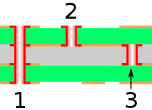
(1) Through hole.
(2) Blind via.
(3) Buried via.
The gray and green layers are nonconducting, while the thin orange layers and vias are conductive.
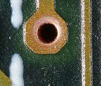
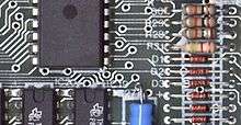
In printed circuit board design, a via consists of two pads in corresponding positions on different layers of the board, that are electrically connected by a hole through the board. The hole is made conductive by electroplating, or is lined with a tube or a rivet. High-density multilayer PCBs may have microvias: blind vias are exposed only on one side of the board, while buried vias connect internal layers without being exposed on either surface. Thermal vias carry heat away from power devices and are typically used in arrays of about a dozen.
A via consists of:
- Barrel — conductive tube filling the drilled hole
- Pad — connects each end of the barrel to the component, plane, or trace
- Antipad — clearance hole between barrel and metal layer to which it is not connected
A via may be at the edge of the board so that it is cut in half when the board is separated; this is known as a castellated hole and is used for a variety of reasons, including allowing one PCB to be soldered to another in a stack.[2]
Three major kinds of vias are shown in right figure. The basic steps of making a PCB are: making the substrate material and stacking it in layers; through-drilling of plating the vias; and copper trace patterning using photolithography and etching. With this standard procedure, possible via configurations are limited to through-holes. Depth-controlled drilling techniques such as using lasers can allow for more varied via types. PCB manufacturing typically starts with a so-called core, a basic double-sided PCB. Layers beyond the first two are stacked from this basic building block. If two more layers are consecutively stacked from bottom of core, you can have a 1-2 via, a 1-3 via and a through hole. Each type of via is made by drilling at each stacking stage. If one layer is stacked on top of the core and other is stacked from the bottom, the possible via configurations are 1-3, 2-3 and through hole. The user must gather information about the PCB manufacturer's allowed methods of stacking and possible vias. For cheaper boards, only through holes are made and antipad (or clearance) is placed on layers which are supposed not to be contacted to vias.
Failure behavior
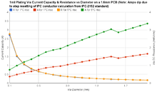
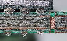
If well made, PCB vias will primarily fail due to differential expansion and contraction between the copper plating and the PCB in the out of plane direction (Z). This differential expansion and contraction will induce cyclic fatigue in the copper plating, eventually resulting in crack propagation and an electrical open. Various design, material, and environmental parameters will influence the rate of this degradation.[3][4]
Gallery

Bottom layer – Red
Top layer – Blue

Above – Top layer
Down – Bottom layer
See also
| The Wikibook Practical Electronics has a page on the topic of: PCB Layout#Holes |
- Through-hole technology (THT)
- Surface-mount technology (SMT)
- Through-silicon via (TSV)
- Via fence
- Feedthrough
References
- ↑ "Plated Through Hole (PTH) Fatigue calculator". DfR Solutions. Retrieved 2017-12-17.
- ↑ "Castellated Holes / Edge Plating PCB / Castellations". Hi-Tech Corp. 2011. Archived from the original on 2016-05-26. Retrieved 2013-01-02.
- ↑ C. Hillman, Understanding plated through via failures, Global SMT & Packaging – November 2013, pp 26-28, https://www.dfrsolutions.com/hubfs/Resources/services/Understanding_Plated_Through_Via_Failures.pdf?t=1514473946162
- ↑ C. Hillman, Reliable Plated Through Via Design and Fabrication, http://resources.dfrsolutions.com/White-Papers/Reliability/Reliable-Plated-Through-Via-Design-and-Fabrication1.pdf
External links
- "Tips for PCB Vias Design" (PDF) (Technical note). Quick-teck. 2014. EN-00417. Retrieved 2017-12-18.
- "Via Tenting - Overview of the variations". WE Online. Würth Elektronik GmbH & Co. KG. 2014. Printed Circuit Boards > Layout > Design Tip > Tenting. Archived from the original on 2017-12-18. Retrieved 2017-12-18.
- "Via Plugging - Overview of the variations". WE Online. Würth Elektronik GmbH & Co. KG. 2014. Printed Circuit Boards > Layout > Design Tip > Plugging. Archived from the original on 2017-12-18. Retrieved 2017-12-18.
- "Via Filling - Overview of the variations". WE Online. Würth Elektronik GmbH & Co. KG. 2013. Printed Circuit Boards > Layout > Design Tip > Filling. Archived from the original on 2017-12-18. Retrieved 2017-12-18.
- "Microvia Filling". WE Online. Würth Elektronik GmbH & Co. KG. 2015. Printed Circuit Boards > Layout > Design Tip > Microvia Filling. Archived from the original on 2017-12-18. Retrieved 2017-12-18.
- Dingler, Klaus; Musewski, Markus (2009-03-18). "Pluggen / Plugging". FED-Wiki (in German). Berlin, Germany: Fachverband Elektronik-Design e.V. (FED). Archived from the original on 2017-12-18. Retrieved 2017-12-18.
- "Via Optimization Techniques for High-Speed Channel Designs" (PDF) (Application note). 1.0. Altera Corporation. May 2008. AN-529-1.0. Archived (PDF) from the original on 2017-12-18. Retrieved 2017-12-18.
- Chu, Jun (2017-04-11). "Controlled Depth Drilling, or Back Drilling". Online Documentation for Altium Products. Altium. Archived from the original on 2017-12-18. Retrieved 2017-12-18.
- Loughhead, Phil (2017-05-30). "Removing Unused Pads and Adding Teardrops". Online Documentation for Altium Products. Altium. Archived from the original on 2017-12-18. Retrieved 2017-12-18.
- Brooks, Douglas G.; Adam, Johannes (2017-02-09), PCB Trace and Via Temperatures: The Complete Analysis (2nd ed.), CreateSpace Independent Publishing Platform, ISBN 978-1541213524