Serial presence detect
In computing, serial presence detect (SPD) is a standardized way to automatically access information about a memory module. Earlier 72-pin SIMMs included five pins that provided five bits of parallel presence detect (PPD) data, but the 168-pin DIMM standard changed to a serial presence detect to encode much more information.[1]
When an ordinary modern computer is turned on, it starts by doing a power-on self-test (POST). Since about the mid-1990s, this process includes automatically configuring the hardware currently present. SPD is a memory hardware feature that makes it possible for the computer to know what memory is present, and what timings to use to access the memory.
Some computers adapt to hardware changes completely automatically. In most cases, there is a special optional procedure for accessing BIOS parameters, to view and potentially make changes in settings. It may be possible to control how the computer uses the memory SPD data—to choose settings, selectively modify memory timings, or possibly to completely over-ride the SPD data (see overclocking).
Stored information
For a memory module to support SPD, the JEDEC standards require that certain parameters be in the lower 128 bytes of an EEPROM located on the memory module. These bytes contain timing parameters, manufacturer, serial number and other useful information about the module. Devices utilizing the memory automatically determine key parameters of the module by reading this information. For example, the SPD data on an SDRAM module might provide information about the CAS latency so the system can set this correctly without user intervention.
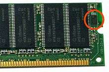
The SPD EEPROM is accessed using SMBus, a variant of the I²C protocol. This reduces the number of communication pins on the module to just two: a clock signal and a data signal. The EEPROM shares ground pins with the RAM, has its own power pin, and has three additional pins (SA0–2) to identify the slot, which are used to assign the EEPROM a unique address in the range 0x50–0x57. Not only can the communication lines be shared among 8 memory modules, the same SMBus is commonly used on motherboards for system health monitoring tasks such as reading power supply voltages, CPU temperatures, and fan speeds.
(SPD EEPROMs also respond to I²C addresses 0x30–0x37 if they have not been write protected, and an extension uses addresses 0x18–0x1F to access an optional on-chip temperature sensor.[2])
SDR SDRAM
The first SPD specification was issued by JEDEC and tightened up by Intel as part of its PC100 memory specification.[3] Most values specified are in binary-coded decimal form. The most significant nibble can contain values from 10 to 15, and in some cases extends higher. In such cases, the encodings for 1, 2 and 3 are instead used to encode 16, 17 and 18. A most significant nibble of 0 is reserved to represent "undefined".
The SPD ROM defines up to three DRAM timings, for three CAS latencies specified by set bits in byte 18. First comes the highest CAS latency (fastest clock), then two lower CAS latencies with progressively lower clock speeds.
| Byte | Bit | Notes | ||||||||
|---|---|---|---|---|---|---|---|---|---|---|
| (dec.) | (hex.) | 7 | 6 | 5 | 4 | 3 | 2 | 1 | 0 | |
| 0 | 0x00 | Number of bytes present | Typically 128 | |||||||
| 1 | 0x01 | log2(size of SPD EEPROM) | Typically 8 (256 bytes) | |||||||
| 2 | 0x02 | Basic memory type (4: SPD SDRAM) | ||||||||
| 3 | 0x03 | Bank 2 row address bits (0–15) | Bank 1 row address bits (1–15) | Bank 2 is 0 if same as bank 1 | ||||||
| 4 | 0x04 | Bank 2 column address bits (0–15) | Bank 1 column address bits (1–15) | Bank 2 is 0 if same as bank 1 | ||||||
| 5 | 0x05 | Number of RAM banks on module (1–255) | Commonly 1 or 2 | |||||||
| 6 | 0x06 | Module data width low byte | Commonly 64, or 72 for ECC DIMMs | |||||||
| 7 | 0x07 | Module data width high byte | 0, unless width ≥ 256 bits | |||||||
| 8 | 0x08 | Interface voltage level of this assembly (not the same as Vcc supply voltage) (0–4) | Decoded by table lookup | |||||||
| 9 | 0x09 | Nanoseconds (0–15) | Tenths of nanoseconds (0.0–0.9) | Clock cycle time at highest CAS latency | ||||||
| 10 | 0x0a | Nanoseconds (0–15) | Tenths of nanoseconds (0.0–0.9) | SDRAM access time from clock (tAC) | ||||||
| 11 | 0x0b | DIMM configuration type (0–2): non-ECC, parity, ECC | Table lookup | |||||||
| 12 | 0x0c | Self | Refresh period (0–5): 64, 256, 128, 32, 16, 8 kHz | Refresh requirements | ||||||
| 13 | 0x0d | Bank 2 2× | Bank 1 primary SDRAM width (1–127, usually 8) | Width of bank 1 data SDRAM devices. Bank 2 may be same width, or 2× width if bit 7 is set. | ||||||
| 14 | 0x0e | Bank 2 2× | Bank 1 ECC SDRAM width (0–127) | Width of bank 1 ECC/parity SDRAM devices. Bank 2 may be same width, or 2× width if bit 7 is set. | ||||||
| 15 | 0x0f | Clock delay for random column reads | Typically 1 | |||||||
| 16 | 0x10 | Page | — | — | — | 8 | 4 | 2 | 1 | Burst lengths supported (bitmap) |
| 17 | 0x11 | Banks per SDRAM device (1–255) | Typically 2 or 4 | |||||||
| 18 | 0x12 | — | 7 | 6 | 5 | 4 | 3 | 2 | 1 | CAS latencies supported (bitmap) |
| 19 | 0x13 | — | 6 | 5 | 4 | 3 | 2 | 1 | 0 | CS latencies supported (bitmap) |
| 20 | 0x14 | — | 6 | 5 | 4 | 3 | 2 | 1 | 0 | WE latencies supported (bitmap) |
| 21 | 0x15 | — | Redundant | Diff. clock | Registered data | Buffered data | On-card PLL | Registered addr. | Buffered addr. | Memory module feature bitmap |
| 22 | 0x16 | — | — | Upper Vcc (supply voltage) tolerance | Lower Vcc (supply voltage) tolerance | Write/1 read burst | Precharge all | Auto-precharge | Early RAS precharge | Memory chip feature support bitmap |
| 23 | 0x17 | Nanoseconds (4–18) | Tenths of nanoseconds (0–9: 0.0–0.9) | Clock cycle time at medium CAS latency | ||||||
| 24 | 0x18 | Nanoseconds (4–18) | Tenths of nanoseconds (0–9: 0.0–0.9) | Data access time from clock (tAC) | ||||||
| 25 | 0x19 | Nanoseconds (1–63) | 0.25 ns (0–3: 0.00–0.75) | Clock cycle time at short CAS latency. | ||||||
| 26 | 0x1a | Nanoseconds (1–63) | 0.25 ns (0–3: 0.00–0.75) | Data access time from clock (tAC) | ||||||
| 27 | 0x1b | Nanoseconds (1–255) | Minimum row precharge time (tRP) | |||||||
| 28 | 0x1c | Nanoseconds (1–255) | Minimum row active–row active delay (tRRD) | |||||||
| 29 | 0x1d | Nanoseconds (1–255) | Minimum RAS to CAS delay (tRCD) | |||||||
| 30 | 0x1e | Nanoseconds (1–255) | Minimum active to precharge time (tRAS) | |||||||
| 31 | 0x1f | 512 MiB | 256 MiB | 128 MiB | 64 MiB | 32 MiB | 16 MiB | 8 MiB | 4 MiB | Module bank density (bitmap). Two bits set if different size banks. |
| 32 | 0x20 | Sign (1: −) | Nanoseconds (0–7) | Tenths of nanoseconds (0–9: 0.0–0.9) | Address/command setup time from clock | |||||
| 33 | 0x21 | Sign (1: −) | Nanoseconds (0–7) | Tenths of nanoseconds (0–9: 0.0–0.9) | Address/command hold time after clock | |||||
| 34 | 0x22 | Sign (1: −) | Nanoseconds (0–7) | Tenths of nanoseconds (0–9: 0.0–0.9) | Data input setup time from clock | |||||
| 35 | 0x23 | Sign (1: −) | Nanoseconds (0–7) | Tenths of nanoseconds (0–9: 0.0–0.9) | Data input hold time after clock | |||||
| 36–61 | 0x24–0x3d | Reserved | For future standardization | |||||||
| 62 | 0x3e | Major revision (0–9) | Minor revision (0–9) | SPD revision level; e.g., 1.2 | ||||||
| 63 | 0x3f | Checksum | Sum of bytes 0–62, not then negated | |||||||
| 64–71 | 0x40–47 | Manufacturer JEDEC id. | Stored little-endian, trailing zero-padded | |||||||
| 72 | 0x48 | Module manufacturing location | Vendor-specific code | |||||||
| 73–90 | 0x49–0x5a | Module part number | ASCII, space-padded | |||||||
| 91–92 | 0x5b–0x5c | Module revision code | Vendor-specific code | |||||||
| 93 | 0x5d | Tens of years (0–9: 0–90) | Years (0–9) | Manufacturing date (YYWW) | ||||||
| 94 | 0x5e | Tens of weeks (0–5: 0–50) | Weeks (0–9) | |||||||
| 95–98 | 0x5f–0x62 | Module serial number | Vendor-specific code | |||||||
| 99–125 | 0x63–0x7f | Manufacturer-specific data | Could be enhanced performance profile | |||||||
| 126 | 0x7e | 0x66 [sic] for 66 MHz, 0x64 for 100 MHz | Intel frequency support | |||||||
| 127 | 0x7f | CLK0 | CLK1 | CLK3 | CLK3 | 90/100 °C | CL3 | CL2 | Concurrent AP | Intel feature bitmap |
DDR SDRAM
The DDR DIMM SPD format is an extension of the SDR SDRAM format. Mostly, parameter ranges are rescaled to accommodate higher speeds.
| Byte | Bit | Notes | ||||||||
|---|---|---|---|---|---|---|---|---|---|---|
| (dec.) | (hex.) | 7 | 6 | 5 | 4 | 3 | 2 | 1 | 0 | |
| 0 | 0x00 | Number of bytes written | Typically 128 | |||||||
| 1 | 0x01 | log2(size of SPD EEPROM) | Typically 8 (256 bytes) | |||||||
| 2 | 0x02 | Basic memory type (7 = DDR SDRAM) | ||||||||
| 3 | 0x03 | Bank 2 row address bits (0–15) | Bank 1 row address bits (1–15) | Bank 2 is 0 if same as bank 1. | ||||||
| 4 | 0x04 | Bank 2 column address bits (0–15) | Bank 1 column address bits (1–15) | Bank 2 is 0 if same as bank 1. | ||||||
| 5 | 0x05 | Number of RAM banks on module (1–255) | Commonly 1 or 2 | |||||||
| 6 | 0x06 | Module data width low byte | Commonly 64, or 72 for ECC DIMMs | |||||||
| 7 | 0x07 | Module data width high byte | 0, unless width ≥ 256 bits | |||||||
| 8 | 0x08 | Interface voltage level of this assembly (not the same as Vcc supply voltage) (0–5) | Decoded by table lookup | |||||||
| 9 | 0x09 | Nanoseconds (0–15) | Tenths of nanoseconds (0.0–0.9) | Clock cycle time at highest CAS latency. | ||||||
| 10 | 0x0a | Tenths of nanoseconds (0.0–0.9) | Hundredths of nanoseconds (0.00–0.09) | SDRAM access time from clock (tAC) | ||||||
| 11 | 0x0b | DIMM configuration type (0–2): non-ECC, parity, ECC | Table lookup | |||||||
| 12 | 0x0c | Self | Refresh period (0–5): 64, 256, 128, 32, 16, 8 kHz | Refresh requirements | ||||||
| 13 | 0x0d | Bank 2 2× | Bank 1 primary SDRAM width (1–127) | Width of bank 1 data SDRAM devices. Bank 2 may be same width, or 2× width if bit 7 is set. | ||||||
| 14 | 0x0e | Bank 2 2× | Bank 1 ECC SDRAM width (0–127) | Width of bank 1 ECC/parity SDRAM devices. Bank 2 may be same width, or 2× width if bit 7 is set. | ||||||
| 15 | 0x0f | Clock delay for random column reads | Typically 1 | |||||||
| 16 | 0x10 | Page | — | — | — | 8 | 4 | 2 | 1 | Burst lengths supported (bitmap) |
| 17 | 0x11 | Banks per SDRAM device (1–255) | Typically 4 | |||||||
| 18 | 0x12 | — | 4 | 3.5 | 3 | 2.5 | 2 | 1.5 | 1 | CAS latencies supported (bitmap) |
| 19 | 0x13 | — | 6 | 5 | 4 | 3 | 2 | 1 | 0 | CS latencies supported (bitmap) |
| 20 | 0x14 | — | 6 | 5 | 4 | 3 | 2 | 1 | 0 | WE latencies supported (bitmap) |
| 21 | 0x15 | — | x | Diff clock | FET switch external enable | FET switch on-board enable | On-card PLL | Registered | Buffered | Memory module feature bitmap |
| 22 | 0x16 | Fast AP | Concurrent auto precharge | Upper Vcc (supply voltage) tolerance | Lower Vcc (supply voltage) tolerance | — | — | — | Includes weak driver | Memory chip feature bitmap |
| 23 | 0x17 | Nanoseconds (0–15) | Tenths of nanoseconds (0.0–0.9) | Clock cycle time at medium CAS latency. | ||||||
| 24 | 0x18 | Tenths of nanoseconds (0.0–0.9) | Hundredths of nanoseconds (0.00–0.09) | Data access time from clock (tAC) | ||||||
| 25 | 0x19 | Nanoseconds (0–15) | Tenths of nanoseconds (0.0–0.9) | Clock cycle time at short CAS latency. | ||||||
| 26 | 0x1a | Tenths of nanoseconds (0.0–0.9) | Hundredths of nanoseconds (0.00–0.09) | Data access time from clock (tAC) | ||||||
| 27 | 0x1b | Nanoseconds (1–63) | 0.25 ns (0–0.75) | Minimum row precharge time (tRP) | ||||||
| 28 | 0x1c | Nanoseconds (1–63) | 0.25 ns (0–0.75) | Minimum row active–row active delay (tRRD) | ||||||
| 29 | 0x1d | Nanoseconds (1–63) | 0.25 ns (0–0.75) | Minimum RAS to CAS delay (tRCD) | ||||||
| 30 | 0x1e | Nanoseconds (1–255) | Minimum active to precharge time (tRAS) | |||||||
| 31 | 0x1f | 512 MiB | 256 MiB | 128 MiB | 64 MiB | 32 MiB | 16 MiB/ 4 GiB | 8 MiB/ 2 GiB | 4 MiB/ 1 GiB | Module bank density (bitmap). Two bits set if different size banks. |
| 32 | 0x20 | Tenths of nanoseconds (0.0–0.9) | Hundredths of nanoseconds (0.00–0.09) | Address/command setup time from clock | ||||||
| 33 | 0x21 | Tenths of nanoseconds (0.0–0.9) | Hundredths of nanoseconds (0.00–0.09) | Address/command hold time after clock | ||||||
| 34 | 0x22 | Tenths of nanoseconds (0.0–0.9) | Hundredths of nanoseconds (0.00–0.09) | Data input setup time from clock | ||||||
| 35 | 0x23 | Tenths of nanoseconds (0.0–0.9) | Hundredths of nanoseconds (0.00–0.09) | Data input hold time after clock | ||||||
| 36–40 | 0x24–0x28 | Reserved | Superset information | |||||||
| 41 | 0x29 | Nanoseconds (1–255) | Minimum active to active/refresh time (tRC) | |||||||
| 42 | 0x2a | Nanoseconds (1–255) | Minimum refresh to active/refresh time (tRFC) | |||||||
| 43 | 0x2b | Nanoseconds (1–63, or 255: no maximum) | 0.25 ns (0–0.75) | Maximum clock cycle time (tCK max.) | ||||||
| 44 | 0x2c | Hundredths of nanoseconds (0.01–2.55) | Maximum skew, DQS to any DQ. (tDQSQ max.) | |||||||
| 45 | 0x2d | Tenths of nanoseconds (0.0–1.2) | Hundredths of nanoseconds (0.00–0.09) | Read data hold skew factor (tQHS) | ||||||
| 46 | 0x2e | Reserved | For future standardization | |||||||
| 47 | 0x2f | — | Height | Height of DIMM module, table lookup | ||||||
| 48–61 | 0x30–0x3d | Reserved | For future standardization | |||||||
| 62 | 0x3e | Major revision (0–9) | Minor revision (0–9) | SPD revision level, 0.0 or 1.0 | ||||||
| 63 | 0x3f | Checksum | Sum of bytes 0–62, not then negated | |||||||
| 64–71 | 0x40–47 | Manufacturer JEDEC id. | Stored little-endian, trailing zero-padded | |||||||
| 72 | 0x48 | Module manufacturing location | Vendor-specific code | |||||||
| 73–90 | 0x49–0x5a | Module part number | ASCII, space-padded | |||||||
| 91–92 | 0x5b–0x5c | Module revision code | Vendor-specific code | |||||||
| 93 | 0x5d | Tens of years (0–90) | Years (0–9) | Manufacturing date (YYWW) | ||||||
| 94 | 0x5e | Tens of weeks (0–50) | Weeks (0–9) | |||||||
| 95–98 | 0x5f–0x62 | Module serial number | Vendor-specific code | |||||||
| 99–127 | 0x63–0x7f | Manufacturer-specific data | Could be enhanced performance profile | |||||||
DDR2 SDRAM
The DDR2 SPD standard makes a number of changes, but is roughly similar to the above. One notable deletion is the confusing and little-used support for DIMMs with two ranks of different sizes.
For cycle time fields (bytes 9, 23, 25 and 49), which are encoded in BCD, some additional encodings are defined for the tenths digit to represent some common timings exactly:
| Hex | Binary | Significance |
|---|---|---|
| A | 1010 | 0.25 (¼) |
| B | 1011 | 0.33 (⅓) |
| C | 1100 | 0.66 (⅔) |
| D | 1101 | 0.75 (¾) |
| E | 1110 | 0.875 (⅞, nVidia XMP extension) |
| F | 1111 | Reserved |
| Byte | Bit | Notes | ||||||||
|---|---|---|---|---|---|---|---|---|---|---|
| Dec | Hex | 7 | 6 | 5 | 4 | 3 | 2 | 1 | 0 | |
| 0 | 0x00 | Number of bytes written | Typically 128 | |||||||
| 1 | 0x01 | log2(size of SPD EEPROM) | Typically 8 (256 bytes) | |||||||
| 2 | 0x02 | Basic memory type (8 = DDR2 SDRAM) | ||||||||
| 3 | 0x03 | Reserved | Row address bits (1–15) | |||||||
| 4 | 0x04 | Reserved | Column address bits (1–15) | |||||||
| 5 | 0x05 | Vertical height | Stack? | ConC? | Ranks−1 (1–8) | Commonly 0 or 1, meaning 1 or 2 | ||||
| 6 | 0x06 | Module data width | Commonly 64, or 72 for ECC DIMMs | |||||||
| 7 | 0x07 | Reserved | ||||||||
| 8 | 0x08 | Interface voltage level of this assembly (not the same as Vcc supply voltage) (0–5) | Decoded by table lookup. Commonly 5 = SSTL 1.8 V | |||||||
| 9 | 0x09 | Nanoseconds (0–15) | Tenths of nanoseconds (0.0–0.9) | Clock cycle time at highest CAS latency. | ||||||
| 10 | 0x0a | Tenths of nanoseconds (0.0–0.9) | Hundredths of nanoseconds (0.00–0.09) | SDRAM access time from clock (tAC) | ||||||
| 11 | 0x0b | DIMM configuration type (0–2): non-ECC, parity, ECC | Table lookup | |||||||
| 12 | 0x0c | Self | Refresh period (0–5): 64, 256, 128, 32, 16, 8 kHz | Refresh requirements | ||||||
| 13 | 0x0d | Primary SDRAM width (1–255) | Commonly 8 (module built from ×8 parts) or 16 | |||||||
| 14 | 0x0e | ECC SDRAM width (0–255) | Width of bank ECC/parity SDRAM devices. Commonly 0 or 8. | |||||||
| 15 | 0x0f | Reserved | ||||||||
| 16 | 0x10 | — | — | — | — | 8 | 4 | — | — | Burst lengths supported (bitmap) |
| 17 | 0x11 | Banks per SDRAM device (1–255) | Typically 4 or 8 | |||||||
| 18 | 0x12 | 7 | 6 | 5 | 4 | 3 | 2 | — | — | CAS latencies supported (bitmap) |
| 19 | 0x13 | Reserved | ||||||||
| 20 | 0x14 | — | — | Mini-UDIMM | Mini-RDIMM | Micro-DIMM | SO-DIMM | UDIMM | RDIMM | DIMM type of this assembly (bitmap) |
| 21 | 0x15 | — | Module is analysis probe | — | FET switch external enable | — | — | — | — | Memory module feature bitmap |
| 22 | 0x16 | — | — | — | — | — | — | — | Includes weak driver | Memory chip feature bitmap |
| 23 | 0x17 | Nanoseconds (0–15) | Tenths of nanoseconds (0.0–0.9) | Clock cycle time at medium CAS latency. | ||||||
| 24 | 0x18 | Tenths of nanoseconds (0.0–0.9) | Hundredths of nanoseconds (0.00–0.09) | Data access time from clock (tAC) | ||||||
| 25 | 0x19 | Nanoseconds (0–15) | Tenths of nanoseconds (0.0–0.9) | Clock cycle time at short CAS latency. | ||||||
| 26 | 0x1a | Tenths of nanoseconds (0.0–0.9) | Hundredths of nanoseconds (0.00–0.09) | Data access time from clock (tAC) | ||||||
| 27 | 0x1b | Nanoseconds (1–63) | 1/4 ns (0–0.75) | Minimum row precharge time (tRP) | ||||||
| 28 | 0x1c | Nanoseconds (1–63) | 1/4 ns (0–0.75) | Minimum row active–row active delay (tRRD) | ||||||
| 29 | 0x1d | Nanoseconds (1–63) | 1/4 ns (0–0.75) | Minimum RAS to CAS delay (tRCD) | ||||||
| 30 | 0x1e | Nanoseconds (1–255) | Minimum active to precharge time (tRAS) | |||||||
| 31 | 0x1f | 512 MiB | 256 MiB | 128 MiB | 16 GiB | 8 GiB | 4 GiB | 2 GiB | 1 GiB | Size of each rank (bitmap). |
| 32 | 0x20 | Tenths of nanoseconds (0.0–1.2) | Hundredths of nanoseconds (0.00–0.09) | Address/command setup time from clock | ||||||
| 33 | 0x21 | Tenths of nanoseconds (0.0–1.2) | Hundredths of nanoseconds (0.00–0.09) | Address/command hold time after clock | ||||||
| 34 | 0x22 | Tenths of nanoseconds (0.0–0.9) | Hundredths of nanoseconds (0.00–0.09) | Data input setup time from strobe | ||||||
| 35 | 0x23 | Tenths of nanoseconds (0.0–0.9) | Hundredths of nanoseconds (0.00–0.09) | Data input hold time after strobe | ||||||
| 36 | 0x24 | Nanoseconds (1–63) | 0.25 ns (0–0.75) | Minimum write recovery time (tWR) | ||||||
| 37 | 0x25 | Nanoseconds (1–63) | 0.25 ns (0–0.75) | Internal write to read command delay (tWTR) | ||||||
| 38 | 0x26 | Nanoseconds (1–63) | 0.25 ns (0–0.75) | Internal read to precharge command delay (tRTP) | ||||||
| 39 | 0x27 | Reserved | Reserved for "memory analysis probe characteristics" | |||||||
| 40 | 0x28 | — | tRC fractional ns (0–5): 0, 0.25, 0.33, 0.5, 0.66, 0.75 | tRFC fractional ns (0–5): 0, 0.25, 0.33, 0.5, 0.66, 0.75 | tRFC + 256 ns | Extension of bytes 41 and 42. | ||||
| 41 | 0x29 | Nanoseconds (1–255) | Minimum active to active/refresh time (tRC) | |||||||
| 42 | 0x2a | Nanoseconds (1–255) | Minimum refresh to active/refresh time (tRFC) | |||||||
| 43 | 0x2b | Nanoseconds (0–15) | Tenths of nanoseconds (0.0–0.9) | Maximum clock cycle time (tCK max) | ||||||
| 44 | 0x2c | Hundredths of nanoseconds (0.01–2.55) | Maximum skew, DQS to any DQ. (tDQSQ max) | |||||||
| 45 | 0x2d | Hundredths of nanoseconds (0.01–2.55) | Read data hold skew factor (tQHS) | |||||||
| 46 | 0x2e | Microseconds (1–255) | PLL relock time | |||||||
| 47–61 | 0x2f–0x3d | Reserved | For future standardization. | |||||||
| 62 | 0x3e | Major revision (0–9) | Minor revision (0.0–0.9) | SPD revision level, usually 1.0 | ||||||
| 63 | 0x3f | Checksum | Sum of bytes 0–62, not negated | |||||||
| 64–71 | 0x40–47 | Manufacturer JEDEC ID | Stored little-endian, trailing zero-pad | |||||||
| 72 | 0x48 | Module manufacturing location | Vendor-specific code | |||||||
| 73–90 | 0x49–0x5a | Module part number | ASCII, space-padded (limited to (,-,), A–Z, a–z, 0–9, space) | |||||||
| 91–92 | 0x5b–0x5c | Module revision code | Vendor-specific code | |||||||
| 93 | 0x5d | Years since 2000 (0–255) | Manufacturing date (YYWW) | |||||||
| 94 | 0x5e | Weeks (1–52) | ||||||||
| 95–98 | 0x5f–0x62 | Module serial number | Vendor-specific code | |||||||
| 99–127 | 0x63–0x7f | Manufacturer-specific data | Could be enhanced performance profile | |||||||
DDR3 SDRAM
The DDR3 SDRAM standard significantly overhauls and simplifies the SPD contents layout. Instead of a number of BCD-encoded nanosecond fields, some "timebase" units are specified to high precision, and various timing parameters are encoded as multiples of that base unit.[7] Further, the practice of specifying different time values depending on the CAS latency has been dropped; now there are just a single set of timing parameters.
Revision 1.1 lets some parameters be expressed as a "medium time base" value plus a (signed, −128 +127) "fine time base" correction. Generally, the medium time base is 1/8 ns (125 ps), and the fine time base is 1, 2.5 or 5 ps. For compatibility with earlier versions that lack the correction, the medium time base number is usually rounded up and the correction is negative. Values that work this way are:
| MTB byte | FTB byte | Value |
|---|---|---|
| 12 | 34 | tCKmin, minimum clock period |
| 16 | 35 | tAAmin, minimum CAS latency time |
| 18 | 36 | tRCDmin, minimum RAS# to CAS# delay |
| 20 | 37 | tRPmin, minimum row precharge delay |
| 21,23 | 38 | tRCmin, minimum active to active/precharge delay |
| Byte | Bit | Notes | ||||||||
|---|---|---|---|---|---|---|---|---|---|---|
| Dec | Hex | 7 | 6 | 5 | 4 | 3 | 2 | 1 | 0 | |
| 0 | 0x00 | Exclude serial from CRC | SPD bytes total (undef/256) | SPD bytes used (undef/128/176/256) | ||||||
| 1 | 0x01 | SPD major revision | SPD minor revision | Typically 1.0 or 1.1 | ||||||
| 2 | 0x02 | Basic memory type (11 = DDR3 SDRAM) | Type of RAM chips | |||||||
| 3 | 0x03 | Reserved | Module type | Type of module; e.g., 2 = Unbuffered DIMM, 3 = SO-DIMM, 11=LRDIMM | ||||||
| 4 | 0x04 | — | Bank address bits−3 | log2(bits per chip)−28 | Zero means 8 banks, 256 Mibit. | |||||
| 5 | 0x05 | — | Row address bits−12 | Column address bits−9 | ||||||
| 6 | 0x06 | Reserved | 1.25 V | 1.35 V | Not 1.5 V | Modules voltages supported. 1.5 V is default. | ||||
| 7 | 0x07 | — | ranks−1 | log2(I/O bits/chip)−2 | Module organization | |||||
| 8 | 0x08 | — | ECC bits (001=8) | log2(data bits)−3 | 0x03 for 64-bit, non-ECC DIMM. | |||||
| 9 | 0x09 | Dividend, picoseconds (1–15) | Divisor, picoseconds (1–15) | Fine Time Base, dividend/divisor | ||||||
| 10 | 0x0a | Dividend, nanoseconds (1–255) | Medium Time Base, dividend/divisor; commonly 1/8 | |||||||
| 11 | 0x0b | Divisor, nanoseconds (1–255) | ||||||||
| 12 | 0x0c | Minimum cycle time tCKmin | In multiples of MTB | |||||||
| 13 | 0x0d | Reserved | ||||||||
| 14 | 0x0e | 11 | 10 | 9 | 8 | 7 | 6 | 5 | 4 | CAS latencies supported (bitmap) |
| 15 | 0x0f | — | 18 | 17 | 16 | 15 | 14 | 13 | 12 | |
| 16 | 0x10 | Minimum CAS latency time, tAAmin | In multiples of MTB; e.g., 80/8 ns. | |||||||
| 17 | 0x11 | Minimum write recovery time, tWRmin | In multiples of MTB; e.g., 120/8 ns. | |||||||
| 18 | 0x12 | Minimum RAS to CAS delay time, tRCDmin | In multiples of MTB; e.g., 100/8 ns. | |||||||
| 19 | 0x13 | Minimum row to row active delay time, tRRDmin | In multiples of MTB; e.g., 60/8 ns. | |||||||
| 20 | 0x14 | Minimum row precharge time, tRPmin | In multiples of MTB; e.g., 100/8 ns. | |||||||
| 21 | 0x15 | tRCmin, bits 11:8 | tRASmin, bits 11:8 | Upper 4 bits of bytes 23 and 22 | ||||||
| 22 | 0x16 | Minimum active to time, tRASmin, bits 7:0 | In multiples of MTB; e.g., 280/8 ns. | |||||||
| 23 | 0x17 | Minimum active to active/refresh, tRCmin, bits 7:0 | In multiples of MTB; e.g., 396/8 ns. | |||||||
| 24 | 0x18 | Minimum refresh recovery delay, tRFCmin, bits 7:0 | In multiples of MTB; e.g., 1280/8 ns. | |||||||
| 25 | 0x19 | Minimum refresh recovery delay, tRFCmin, bits 15:8 | ||||||||
| 26 | 0x1a | Minimum internal write to read delay, tWTRmin | In multiples of MTB; e.g., 60/8 ns. | |||||||
| 27 | 0x1b | Minimum internal read to precharge delay, tRTPmin | In multiples of MTB; e.g., 60/8 ns. | |||||||
| 28 | 0x1c | Reserved | tFAWmin, bits 11:8 | In multiples of MTB; e.g., 240/8 ns. | ||||||
| 29 | 0x1d | Minimum four activate window delay tFAWmin, bits 7:0 | ||||||||
| 30 | 0x1e | DLL-off | — | — | — | — | — | RZQ/7 | RZQ/6 | SDRAM optional features support bitmap |
| 31 | 0x1f | PASR | — | — | — | ODTS | ASR | ETR 1× | ETR (95 °C) | SDRAM thermal and refresh options |
| 32 | 0x20 | Present | Accuracy (TBD; currently 0 = undefined) | DIMM thermal sensor present? | ||||||
| 33 | 0x21 | Nonstd. | Die count | — | — | Signal load | Nonstandard SDRAM device type (e.g., stacked die) | |||
| 34 | 0x22 | tCKmin correction (new for 1.1) | Signed multiple of FTB, added to byte 12 | |||||||
| 35 | 0x23 | tAAmin correction (new for 1.1) | Signed multiple of FTB, added to byte 16 | |||||||
| 36 | 0x24 | tRCDmin correction (new for 1.1) | Signed multiple of FTB, added to byte 18 | |||||||
| 37 | 0x25 | tRPmin correction (new for 1.1) | Signed multiple of FTB, added to byte 20 | |||||||
| 38 | 0x26 | tRCmin correction (new for 1.1) | Signed multiple of FTB, added to byte 23 | |||||||
| 39–59 | 0x27–0x3b | Reserved | For future standardization. | |||||||
| 60 | 0x3c | — | Module height, mm (1–31, >45) | Module nominal height | ||||||
| 61 | 0x3d | Back thickness, mm (1–16) | Front thickness, mm (1–16) | Module thickness, value = ceil(mm) − 1 | ||||||
| 62 | 0x3e | Design | Revision | JEDEC design number | JEDEC reference design used (11111=none) | |||||
| 63–116 | 0x3f–0x74 | Module-specific section | Differs between registered/unbuffered | |||||||
| 117 | 0x75 | Module manufacturer ID, lsbyte | Assigned by JEP-106 | |||||||
| 118 | 0x76 | Module manufacturer ID, msbyte | ||||||||
| 119 | 0x77 | Module manufacturing location | Vendor-specific code | |||||||
| 120 | 0x78 | Tens of years | Years | Manufacturing year (BCD) | ||||||
| 121 | 0x79 | Tens of weeks | Weeks | Manufacturing week (BCD) | ||||||
| 122–125 | 0x7a–0x7d | Module serial number | Vendor-specific code | |||||||
| 126–127 | 0x7e–0x7f | SPD CRC-16 | Includes bytes 0–116 or 0–125; see byte 0 bit 7 | |||||||
| 128–145 | 0x80–0x91 | Module part number | ASCII subset, space-padded | |||||||
| 146–147 | 0x92–0x93 | Module revision code | Vendor-defined | |||||||
| 148–149 | 0x94–0x95 | DRAM manufacturer ID | As distinct from module manufacturer | |||||||
| 150–175 | 0x96–0xAF | Manufacturer-specific data | ||||||||
The memory capacity of a module can be computed from bytes 4, 7 and 8. The module width (byte 8) divided by the number of bits per chip (byte 7) gives the number of chips per rank. That can then be multiplied by the per-chip capacity (byte 4) and the number of ranks of chips on the module (usually 1 or 2, from byte 7).
Extensions
The JEDEC standard only specifies some of the SPD bytes. The truly critical data fits into the first 64 bytes,[5][6][9][10][11] while some of the remainder is earmarked for manufacturer identification. However, a 256-byte EEPROM is generally provided. A number of uses have been made of the remaining space.
Enhanced Performance Profiles (EPP)
Memory generally comes with conservative timing recommendations in the SPD ROM, to ensure basic functionality on all systems. Enthusiasts often spend considerable time manually adjusting the memory timings for higher speed.
Enhanced Performance Profiles is an extension of SPD, developed by Nvidia and Corsair, which includes additional information for higher-performance operation of DDR2 SDRAM, including supply voltages and command timing information not included in the JEDEC SPD spec. The EPP information is stored in the same EEPROM, but in bytes 99-127, which are unused by standard DDR2 SPD.[12]
| Bytes | Size | Full profiles | Abbreviated profiles |
|---|---|---|---|
| 99–103 | 5 | EPP header | |
| 104–109 | 6 | Profile FP1 | Profile AP1 |
| 110–115 | 6 | Profile AP2 | |
| 116–121 | 6 | Profile FP2 | Profile AP3 |
| 122–127 | 6 | Profile AP4 | |
The parameters are particularly designed to fit the memory controller on the nForce 5, nForce 6 and nForce 7 chipsets. Nvidia encourages support for EPP in the BIOS for its high-end motherboard chipsets. This is intended to provide "one-click overclocking" to get better performance with minimal effort.
Nvidia's name for EPP memory that has been qualified for performance and stability is "SLI-ready memory".[13] The term "SLI-ready-memory" has caused some confusion, as it has nothing to do with SLI video. One can use EPP/SLI memory with a single video card (even a non-Nvidia card), and one can run a multi-card SLI video setup without EPP/SLI memory.
An extended version, EPP 2.0, supports DDR3 memory as well.[14]
Extreme Memory Profile (XMP)
A similar, Intel-developed JEDEC SPD extension for DDR3 SDRAM DIMMs. This uses bytes 176–255, which are unallocated by JEDEC, to encode higher-performance memory timings.[15]
| Bytes | Size | Use |
|---|---|---|
| 176–184 | 10 | XMP header |
| 185–219 | 33 | XMP profile 1 ("enthusiast" settings) |
| 220–254 | 36 | XMP profile 2 ("extreme" settings) |
The header contains the following data. Most importantly, it contains a "medium timebase" value MTB, as a rational number of nanoseconds (common values are 1/8, 1/12 and 1/16 ns). Many other later timing values are expressed as an integer number of MTB units.
Also included in the header is the number of DIMMs per memory channel that the profile is designed to support; including more DIMMs may not work well.
| Byte | Bits | Use |
|---|---|---|
| 176 | 7:0 | XMP magic number byte 1 0x0C |
| 177 | 7:0 | XMP magic number byte 2 0x4A |
| 178 | 0 | Profile 1 enabled (if 0, disabled) |
| 1 | Profile 2 enabled | |
| 3:2 | Profile 1 DIMMs per channel (1–4 encoded as 0–3) | |
| 5:4 | Profile 2 DIMMs per channel | |
| 7:6 | Reserved | |
| 179 | 3:0 | XMP minor version number (x.0 or x.1) |
| 7:4 | XMP major version number (0.x or 1.x) | |
| 180 | 7:0 | Medium timebase dividend for profile 1 |
| 181 | 7:0 | Medium timebase divisor for profile 1 (MTB = dividend/divisor ns) |
| 182 | 7:0 | Medium timebase dividend for profile 2 (e.g. 8) |
| 183 | 7:0 | Medium timebase divisor for profile 2 (e.g. 1, giving MTB = 1/8 ns) |
| 184 | 7:0 | Reserved |
| Byte 1 | Byte 2 | Bits | Use |
|---|---|---|---|
| 185 | 220 | 0 | Module Vdd voltage twentieths (0.00 or 0.05) |
| 4:1 | Module Vdd voltage tenths (0.0–0.9) | ||
| 6:5 | Module Vdd voltage units (0–2) | ||
| 7 | Reserved | ||
| 186 | 221 | 7:0 | Minimum SDRAM clock period tCKmin (MTB units) |
| 187 | 222 | 7:0 | Minimum CAS latency time tAAmin (MTB units) |
| 188 | 223 | 7:0 | CAS latencies supported (bitmap, 4–11 encoded as bits 0–7) |
| 189 | 224 | 6:0 | CAS latencies supported (bitmap, 12–18 encoded as bits 0–6) |
| 7 | Reserved | ||
| 190 | 225 | 7:0 | Minimum CAS write latency time tCWLmin (MTB units) |
| 191 | 226 | 7:0 | Minimum row precharge delay time tRPmin (MTB units) |
| 192 | 227 | 7:0 | Minimum RAS to CAS delay time tRCDmin (MTB units) |
| 193 | 228 | 7:0 | Minimum write recovery time tWRmin (MTB units) |
| 194 | 229 | 3:0 | tRASmin upper nibble (bits 11:8) |
| 7:4 | tRCmin upper nibble (bits 11:8) | ||
| 195 | 230 | 7:0 | Minimum active to precharge delay time tRASmin bits 7:0 (MTB units) |
| 196 | 231 | 7:0 | Minimum active to active/refresh delay time tRCmin bits 7:0 (MTB units) |
| 197 | 232 | 7:0 | Maximum average refresh interval tREFI lsbyte (MTB units) |
| 198 | 233 | 7:0 | Maximum average refresh interval tREFI msbyte (MTB units) |
| 199 | 234 | 7:0 | Minimum refresh recovery delay time tRFCmin lsbyte (MTB units) |
| 200 | 235 | 7:0 | Minimum refresh recovery delay time tRFCmin msbyte (MTB units) |
| 201 | 236 | 7:0 | Minimum internal read to precharge command delay time tRTPmin (MTB units) |
| 202 | 237 | 7:0 | Minimum row active to row active delay time tRRDmin (MTB units) |
| 203 | 238 | 3:0 | tFAWmin upper nibble (bits 11:8) |
| 7:4 | Reserved | ||
| 204 | 239 | 7:0 | Minimum four activate window delay time tFAWmin bits 7:0 (MTB units) |
| 205 | 240 | 7:0 | Minimum internal write to read command delay time tWTRmin (MTB units) |
| 206 | 241 | 2:0 | Write to read command turnaround time adjustment (0–7 clock cycles) |
| 3 | Write to read command turnaround adjustment sign (0=pull-in, 1=push-out) | ||
| 6:4 | Read to write command turnaround time adjustment (0–7 clock cycles) | ||
| 7 | Read to write command turnaround adjustment sign (0=pull-in, 1=push-out) | ||
| 207 | 242 | 2:0 | Back-to-back command turnaround time adjustment (0–7 clock cycles) |
| 3 | Back-to-back turnaround adjustment sign (0=pull-in, 1=push-out) | ||
| 7:4 | Reserved | ||
| 208 | 243 | 7:0 | System CMD rate mode. 0=JTAG default, otherwise in peculiar units of MTB × tCK/ns. E.g. if MTB is 1/8 ns, then this is in units of 1/8 clock cycle. |
| 209 | 244 | 7:0 | SDRAM auto self refresh performance. Standard version 1.1 says documentation is TBD. |
| 210–218 | 245–253 | 7:0 | Reserved |
| 219 | 254 | 7:0 | Reserved, vendor-specific personality code. |
Vendor-specific memory
A common misuse is to write information to certain memory regions to bind vendor-specific memory modules to a specific system. Fujitsu Technology Solutions is known to do this. Adding different memory module to the system usually results in a refusal or other counter-measures (like pressing F1 on every boot).
02 0E 00 01-00 00 00 EF-02 03 19 4D-BC 47 C3 46 ...........M.G.F
53 43 00 04-EF 4F 8D 1F-00 01 70 00-01 03 C1 CF SC...O....p.....
This is the output of a 512 MB memory module from Micron Technologies, branded for Fujitsu-Siemens Computers, note the "FSC" string. The system BIOS rejects memory modules that don't have this information starting at offset 128h.
Reading and writing SPD information
Memory module manufacturers write the SPD information to the EEPROM on the module. Motherboard BIOSes read the SPD information to configure the memory controller. There exist several programs that are able to read and modify SPD information on most, but not all motherboard chipsets.
- dmidecode program that can decode information about memory (and other things) and runs on Linux, FreeBSD, NetBSD, OpenBSD, BeOS, Cygwin and Solaris. dmidecode does not access SPD information directly; it reports the BIOS data about the memory.[17] This information may be limited or incorrect.
- On Linux systems, the user space program decode-dimms[18] provided with i2c-tools [19] decodes and prints information on any memory with SPD information in the computer. It requires SMBus controller support in the kernel, the EEPROM kernel driver, and also that the SPD EEPROMs are connected to the SMBus. On older Linux distributions, decode-dimms.pl was available as part of lm_sensors.
- OpenBSD has included a driver (spdmem(4)) since version 4.3 to provide information about memory modules. The driver was ported from NetBSD, where it is available since release 5.0.
- Coreboot reads and uses SPD information to initialize all memory controllers in a computer with timing, size and other properties.
- Windows systems use programs like HWiNFO32,[20] CPU-Z and Speccy, which can read and display DRAM module information from SPD.
Chipset-independent reading and writing of SPD information is done by accessing the memory's EEPROM directly with eeprom programmer hardware and software.
A not so common use for old laptops is as generic SMBus readers, as the internal EEPROM on the module can be disabled once the BIOS has read it so the bus is essentially available for use. The method used is to pull low the A0,A1 lines so the internal memory shuts down, allowing the external device to access the SMBus. Once this is done, a custom Linux build or DOS application can then access the external device. A common use is recovering data from LCD panel memory chips to retrofit a generic panel into a proprietary laptop.
On older equipment
Some older equipment require the use of SIMMs with parallel presence detect (more commonly called simply presence detect or PD). Some of this equipment uses non-standard PD coding, IBM computers and Hewlett-Packard LaserJet and other printers in particular.
See also
References
- ↑ Thomas P. Koenig; Nathan John (1997-02-03), "Serial Presence Detection poised for limelight", Electronic News, 43 (2153)
- ↑ JEDEC Standard 21-C section 4.1.4 "Definition of the TSE2002av Serial Presence Detect (SPD) EEPROM with Temperature Sensor (TS) for Memory Module Applications"
- ↑ Application note INN-8668-APN3: SDRAM SPD Data Standards, memorytesters.com
- ↑ PC SDRAM Serial Presence Detect (SPD) Specification (PDF), 1.2A, December 1997, p. 28
- 1 2 JEDEC Standard 21-C section 4.1.2.4 "SPDs for DDR SDRAM"
- 1 2 JEDEC Standard 21-C section 4.1.2.10 "Specific SPDs for DDR2 SDRAM"
- ↑ Understanding DDR3 Serial Presence Detect (SPD) Table
- ↑ JESD21-C Annex K: Serial Presence Detect for DDR3 SDRAM Modules, Release 4, SPD Revision 1.1
- ↑ JEDEC Standard 21-C section 4.1.2.11 "Serial Presence Detect (SPD) for DDR3 SDRAM Modules"
- ↑ JEDEC Standard 21-C section 4.1.2 "SERIAL PRESENCE DETECT STANDARD, General Standard"
- ↑ JEDEC Standard 21-C section 4.1.2.5 "Specific PDs for Synchronous DRAM (SDRAM)"
- ↑ DDR2 UDIMM Enhanced Performance Profiles Design Specification (PDF), Nvidia, 2006-05-12, retrieved 2009-05-05
- ↑ http://www.nvidia.com/docs/CP/45121/sli_memory.pdf
- ↑ Enhanced Performance Profiles 2.0 (pages 2–3)
- ↑ Intel Extreme Memory Profile (Intel XMP) DDR3 Technology
- 1 2 3 Intel® Extreme Memory Profile (XMP) Specification, Rev 1.1 (PDF), October 2007, archived from the original (PDF) on 2012-03-06, retrieved 2010-05-25
- ↑ dmidecode: What's it good for?
- ↑ "Archived copy". Archived from the original on 2 December 2008. Retrieved 2009-07-16. decode-dimms Perl program
- ↑ "I2CTools – lm-sensors". Lm-sensors.org. Archived from the original on 11 March 2012. Retrieved 14 August 2014.
- ↑ HWiNFO32
External links
- Serial Presence Detect Standard, General Standard
- SPD Rev1.0 for DDR SDRAM
- SPD Rev1.2 for DDR2 SDRAM
- SPD Rev1.3 for DDR2 SDRAM
- SPECIALITY DDR2-1066 SDRAM
- Linux package i2c-tools
- Instructions on how to use lm-sensors or i2c-tools to read the data
- Memory Performance: 16GB DDR3-1333 to DDR3-2400 on Ivy Bridge IGP with G.Skill – explanation of various timing values