NEC V60
 Die shot of NEC V60 microprocessor Name "V60 D70616" in bottom center | |
| Produced |
V60: 1986 V70: 1987 V80: 1989 AFPP: 1989 |
|---|---|
| Common manufacturer(s) | |
| Max. CPU clock rate |
V60: 16 MHz V70: 20/25 MHz V80: 25/33 MHz AFPP: 20 MHz |
| Min. feature size |
V60: 1.5/1.2 μm V70: 1.5/1.2 μm V80: 0.8 μm AFPP: 1.2 μm |
| Instruction set | NEC V60-V80[1] |
| Microarchitecture | "V60/V70", "V80" |
| L1 cache | V80: 1K/1K |
| Transistors |
V60: 375K V70: 385K V80: 980K AFPP: 433K |
| Instructions |
V60/V70: 119 V80: 123 |
| Extensions |
|
| Data width |
V60: 16 (int. 32) V70: 32 V80: 32 |
| Address width |
V60: 24 (int. 32) V70: 32 V80: 32 |
| Virtual address width | 32 Linear[1] |
| Predecessor | V20-V50 |
| Successor | V800 Series |
| Application |
Embedded, Minicomputer, Game arcade |
| Co-processor | AFPP (μPD72691) |
| Package(s) | |
| Product code name(s) |
|
NEC V60[1][2] is a CISC microprocessor once manufactured by NEC started in 1986. It has MMU, and RTOS supports both for Unix-based user-application-oriented systems[3] and for I‑TRON based hardware-control-oriented embedded systems. This article also describes V70 and V80 because these have the same ISA as V60.[4] In addition, dedicated co-FPP,[5] multi-cpu lockstep fault-tolerant mechanism named FRM, development tools including Ada certified system MV‑4000, and ICE are described. At last, their successor[6] the V800 Series product families are briefly introduced.
V60/V70/V80's application covered much wide area, including: circuit switching telephone exchanges, minicomputers, aerospace guidance systems,[7] word processors, industrial computers, and various game arcades.
Nowadays, CPU simulator software has been kept providing by the MAME development team, to emulate old games for enthusiasts. The latest open-source code is available from GitHub repository (<mamedev/mame></src/devices/cpu/v60/>).
Introduction
NEC V60[2][1] is a CISC[8] processor once manufactured by NEC started in 1986.[9] It is the first 32-bit general-purpose microprocessor commercially available in Japan.[10]
Based on a relatively traditional design at that moment,[11][12][13][14][15] indeed it was a radical divorcing from NEC's previous 16-bit V–Series; the V20-V50.[16] Those were based on the Intel 8086 model.[8] But V60 still retained the ability to emulate V20/V30.[1]:§10 According to NEC's documentation, this computer architectural change was made due to the increasing demands for, and the diversity of, high-level programming languages. Such trend called for a processor both with performance; doubling buses width to 32 bits, and with flexibility; having large numbers of general-purpose registers.[2][1] These were a part of common features of Reduced Instruction Set Computer.[17] This transition from CISC to RISC brought much benefits to the emerging markets — at that moment.
But today, both of two Silicon Valley born RISCs are pressed, instead Intel's x86 has been main stream for these decades. The reason is, though x86 has CISC ISA, 80486 internally adopts RISC features.[18][19] According to Pat Gelsinger's word, binary backward compatibility for the legacy software assets is much important than ISA change.[20]
Overview
Instruction set
The V60 (μPD70616) /.mu.PD70616/, however, staid in CISC features.[21] Its manual describes them as mainframe-computer-based fully orthogonal instruction set, in other words, Complex Instruction Set Computer, which comprises; non-uniform length instructions, memory-to-memory operations including string manipulation, and fairly complex operand addressing schemes.[1][2][17]
Family
The V60 has 32 bits internal buses although it has externally narrower 16 bits data and 24 bits address buses. In addition, V60 has 32 of 32-bit general-purpose registers.[1]:§1 Its basic architecture is inherited to the following models. The V70 (μPD70632) has 32 bits external buses, released in 1987. Launched in 1989, the V80 (μPD70832)[4] is the culmination of the series; having on-chip caches, having a branch predictor, and less reliance on microcode for complex operations.[22]
Software
The operating systems, developed for the V60-V80 series, are generally oriented toward real-time operations. Several OSs were ported on them, including real-time Unix and real-time I‑TRON.[23][24]
Because the V60/V70 has been used for various Japanese game arcades, their instruction set architecture is still surviving as the CPU simulator, called MAME, Multiple Arcade Machine Emulator, for this niche.[25] The latest open-source code is available from GitHub repository (<mamedev/mame></src/devices/cpu/v60/>).
FRM
All three processors has the synchronous multiple modular lockstep mechanism named FRM (Functional Redundancy Monitoring), which enables fault-tolerant computer systems. It requires plural of devices of the same model, then one of them becomes the "master mode," while the other devices listen to the master device in the "checker mode." If two or more devices arise different result via their "fault output" pins simultaneously, the majority voting decision can be made by external circuits. In addition, recovery method, either with roll-back by "retry" or with roll-forward by "exception" for the instruction which is detected mismatch, can be selected via an external pin.[26][27][1]:§11[4][28][29]:§3-229, 266
| Pin Name | I/O | Function |
|---|---|---|
| BMODE (FRM) | Input | Select the normal bus (master) mode or FRM operating (checker) mode |
| BLOCK (MSMAT) | Output | Master output requesting bus lock, i.e. freezing bus operation Checker output indicating a mismatch has been detected |
| BFREZ | Input | Assertion for freezing bus operation |
| RT/EP | Input | Selecting input for "roll-back by retry" or "roll-forward by exception" |
V60
The work on V60 processor began in 1982 under the leadership of Yoichi Yano.[30] About 250 engineers participated and the V60 (μPD70616) debuted in February 1986.[31] It had a six-stage pipeline, built-in memory management unit and floating-point arithmetic. It was manufactured in 1.5 μm on a two-layer aluminum metal CMOS process using 375,000 transistors on a 13.9 × 13.8 mm2 die.[9][32] It operated at 5 V and was initially packaged in a 68-pin PGA.[33] The first version ran at 16 MHz and attained 3.5 MIPS.[32] Its sample price at launch was set to ¥100,000 ($588.23). It entered full-scale production in August 1986.[32]
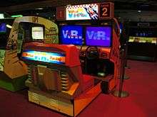
Sega employed this processor for the most of its arcade game sets in the 1990s; both the Sega System 32 and the Sega Model 1 architectures used V60 for their main CPU. (The latter one used lower-cost variant μPD70615 /.mu.PD70615/,[34] which doesn't implement V20/V30 emulation and FRM.[35] ) The V60 was also used for the main CPU in the SSV arcade architecture—so named because it was developed together by Seta, Sammy, and Visco.[36] Sega originally considered using a 16 MHz V60 as the basis for its Sega Saturn console, but after receiving the word, that the PlayStation employed a MIPS R3000A at 33.8 MHz processor, instead chose the dual-SH-2 design for the eventual production model.[37]
In 1988, NEC released a kit called PS98-145-HMW for Unix enthusiasts. The kit contained a V60 processor board that could be plugged into selected models of the PC-9800 computer series and a '15 8"-floppy disks distribution' of their UNIX System V port, the PC-UX/V Rel 2.0 (V60) (refer to external link below). The suggested retail price for this kit was 450,000 Yen.[38] NEC group companies themselves intensively employed V60 processor. Their telephone circuit switcher (exchanger), which was one of the first intended target, used V60. In 1991, they expanded word processor products line, named "Bungou Mini" (文豪ミニ in Japanese) series 5SX, 7SX, and 7SD, with a V60 for fast outline font processing, while the main system processor was a 16 MHz NEC V33 (Bungou Mini 5RX with "high speed outline font smoothing" TV CM on YouTube).[39] In addition, V60 has microcode variants for NEC's minicomputer MS-4100 Series, which was the fastest one in Japan at that moment.[40][41][42]
V70
The V70 (μPD70632) /.mu.PD70632/ improved on V60 by widening external buses to 32 bits, then both internal and external buses became 32 bits width. It was also manufactured in a 1.5 μm with two-metal layer process. Its 14.35 × 14.24 mm2 die had 385,000 transistors and was packaged in a 132-pin ceramic PGA. Its MMU had support for demand paging. Its floating-point unit claimed IEEE 754 compliance.[28] The 20 MHz version attained a peak performance of 6.6 MIPS and was priced at launch in August 1987 at ¥100,000 ($719.42). Initial production capacity was 20,000 units monthly.[43] A later report describes it as fabricated in 1.2-micrometer CMOS and 12.23 × 12.32 mm2 die.[4] The V70 had a two-cycle non-pipeline (T1-T2) external bus system, whereas that of the V60 operated at 3 or 4 cycles (T1-T3/T4).[4][2] Of course, the internal units were pipelined.
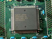
V70 was used by Sega in its System Multi 32 design [44] and by Jaleco in its Mega System 32 design. (See the top photo of the V70, which is mounted on the latter system's printed circuit board.)[45]
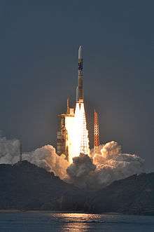
The "aerospace-spec" (JAXA formerly NASDA qualified EEE grade) variant of V70, running with RX616, was embedded in the main control module called Guidance Control Computer by JAXA into the H‑IIA carrier rockets, and satellites such as Akatsuki (Venus Climate Orbiter) and Kibo (ISS module).[7][46][47] It had been used until their replacement in 2013 flight 22 with the 64-bit microprocessor HR5000, which is based on MIPS64-5Kf architecture,[48] fabricated by HIREC.[49][50][51] The H‑IIA type launch vehicles deployed domestically in Japan, although JAXA called for satellites as its payload from the foreign countries. As is described in JAXA's LSI (MPU/ASIC) roadmap, this V70 variant is "32bit MPU (H32/V70)" which development term, probably including QT phase, was "from the middle of 1980's to early 1990's." In addition, the HR5000 is "64bit MPU (25MHz)," which development is completed around 2011. Then V70 was retired.[52]:9[53]
"Space Environment Data Acquisition" for the V70 was done by Kibo-ISS exposed facility.
| Item | Part No. | SEE (Single Event Effect) Monitored Item |
Result [54] |
|---|---|---|---|
| V70-MPU | NASDA 38510/92101xz | SEU (Single Event Upset) SEL (Single Event Latch-up) | Not observed (—2010/9/30) |
V80
The V80 (μPD70832) /.mu.PD70832/[4] was launched in the spring of 1989. By incorporating on-chip caches and a branch predictor, it was declared NEC's 486 by Computer Business Review.[55][56] The performance of V80 was two to four times than that of V70, depending on application. For example, compared with V70, the V80 had a 32-bit hardware multiplier to reduce integer multiplication cycles to 9 from 23. (For more detailed differences, see hardware architecture section below.) The V80 was manufactured in 0.8-micrometer CMOS process with a die area of 14.49 × 15.47 mm2 consisting of 980,000 transistors. It was packaged in a 280-pin PGA, and operated at 25 and 33 MHz with claimed peak performance of 12.5 and 16.5 MIPS, respectively. V80 had separated 1 KB on-die cache both for instructions and for data, and had 64-entry branch predictor; the performance gain, attributed to the latter, was about 5%. The launch prices of V80 were cited as equivalent to $1200 for the 33 MHz model and $960 for the 25 MHz model. Supposedly a 45 MHz model was scheduled for 1990,[56] but did not materialize.
The V80, associated with μPD72691 co-FPP and μPD71101 simple peripheral chips, was used for industrial computer with the RX-UX832 real-time UNIX and a X11-R4 based window system.[57][58]
AFPP (co‑FPP)
The AFPP (μPD72691) /.mu.PD72691/ is a co-processor for floating point arithmetic operations.[59] The name stands for Advanced Floating Point Processor as is described in NEC's data sheet. The V60/V70/V80 themselves can perform floating point arithmetic, but they are very slow because of microcode operations without dedicated hardware. In 1989, to compensate V60/V70/V80 for their fairly weak floating point performance, NEC launched the 80-bit floating point co-processor; for 32-bit single precision, for 64-bit double precision, and for 80-bit extended precision IEEE 754 format operations.[5][4] This chip claimed 6.7 MFLOPS in the vector-matrix multiplication, operating at 20 MHz. It was fabricated in 1.2-micrometer double-metal layer CMOS process containing 433,000 transistors on an 11.6 × 14.9 mm2 die.[5] It was packaged in a 68-pin PGA. This co-processor connected to V80 via the dedicated bus. But in case of connecting to V60 and V70, it shared their main buses, which scenario diminished their peak performance.[4]
Hardware Architecture
V60/V70/V80 shared the basic architecture. They had thirty-two 32-bit general-purpose registers, although the last three of them were commonly used as stack pointer, frame pointer, and argument pointer, those were well matched with high level language compilers' calling conventions.[28][60] The V60 and V70 had a 119-instruction set,[28] slightly extended to 123 instructions for the V80. The instructions have non-uniform length between one and 22 bytes,[1] and they take two operands, both of which can be memory locations.[4] After studying the V60's reference manual, Paul Vixie described it as "a very VAX-ish arch, with a V20/V30 emulation mode (which, if you recall, means it can run Intel 8086/8088 software)".[61]
V60-V80 had a built-in MMU[9][59] that divide the 4 GB virtual address space into in four 1-GB sections, each section further divided in 1,024 1-MB areas, each area composed of 256 4-KB pages. On the V60/V70 four registers (ATBR0 to ATBR3) store section pointers on the processor, but the area tables entries (ATE) and page tables entries (PTE) are stored into off-chip RAM. The V80 merged the ATE and ATBR registers, which are both on-chip with only the PTE entries stored into external RAM, allowing for a faster execution of TLB misses by eliminating one memory read.[4]
The TLBs on the V60/70 are 16-entry fully associative with replacement done by microcode. The V80 in contrast has a 64-entry 2-way set associative TLB with replacement done in hardware. TLB replacement took 58 cycles in the V70 and also disrupted the pipelined execution of other instructions. On the V80 a TLB replacement took only 6/11 cycles depending if the page was in the same area or not; pipeline disruption no longer occurred in V80 because of the separate TLB replacement hardware unit which operated in parallel to the rest of the processor.[4]
All three processors used the same protection mechanism with 4 execution levels (set via a program status word), with ring 0 being the privileged level that could access a special set of privileged registers on the processors.[4]
All three models supported a triple-mode redundancy configuration with three CPUs used in a byzantine fault tolerance scheme with bus freeze, instruction retry, and chip replacement signals.[4][27] The V80 also added parity signals to its data and address buses.[4]
String operations were implemented in microcode in the V60/V70, but aided by hardware Data Control Unit in the V80, running at full bus speed. This made string operations about five times faster in the V80.[4]
All floating point operations are largely implemented in microcode across the family and thus and are fairly slow. On the V60/V70 the 32-bit floating point operations took 120/116/137 cycles for addition/multiplication/division, while the corresponding 64-bit floating point operations took 178/270/590 cycles. The V80 had some limited hardware assist for parts of the floating point operations, e.g. decomposition into sign, exponent and mantissa, thus its floating point unit was claimed up to 3 times as effective as the one of the V70, with 32-bit operations taking 36/44/74 cycles while 64-bit floating point operations taking 75/110/533 cycles on the V80 (again, for addition/multiplication/division).[4]
Operating Systems
Unix (non-real-time and real-time)
NEC ported several variants of Unix to its V60/V70/V80 processors for user-application-oriented systems, including real-time ones. The first flavor of NEC's UNIX System V port for V60 was called PC-UX/V Rel 2.0 (V60).[62] (also refer to external link photos below, much interesting) NEC also developed a variant for V60/V70/V80 with a focus on real-time operation called Real-time UNIX RX-UX 832.[3] It has double layered kernel structure, and all the kernel call of Unix issues task to the real-time kernel. The multiprocessor version of RX-UX 832 was also developed, and was named MUSTARD (A Multiprocessor Unix for Embedded Real-Time Systems).[63] The MUSTARD-powered computer prototype used eight V70 processors. It utilize FRM function, and can configure and change the structure of master and checker upon request.[64] (Google Books)
I‑TRON (real-time)
For hardware-control-oriented embedded systemss, the I‑TRON based real-time operating system, named RX616, was implemented by NEC for the V60/V70.[26][23] The 32-bit RX616 was a continuous fork from the 16-bit RX116, which was for the V20-V50.[43][24]
FlexOS (real-time)
In 1987, Digital Research, Inc. had also announced that they were planning on porting FlexOS to the V60 and V70.[65]
CP/M and DOS (legacy 16-bit)
The V60 could also run CP/M and DOS programs (ported from the V20-V50 series) using V20/V30 emulation mode.[32] According to a 1991 article in InfoWorld, Digital Research was working on a version of Concurrent DOS for the V60 at some point, but this was never released as the V60/V70 processors were not imported in the US for use in PC clones.[66]
Development Tools
C/C++ cross compilers
Regarding the development tool kit and IDE, NEC had its own C compiler the PKG70616; "Software Generation tool package for V60/V70."[67] In addition, GHS (Green Hills Software) made its native mode C compiler (MULTI), and MetaWare, Inc.[68] (currently Synopsys, via ARC International) made one for V20/V30 emulation mode, i.e. 8086 model, called High C/C++.[69][19]:acknowledgement Cygnus Solutions (currently Red Hat) also ported GCC in a part of EGCS fork,[70] but it seems not to be public.[71][72]
As of 2018, the machine directory necv70 is still kept alive in the newlib C language libraries (libc.a and libm.a) by RedHat.[73] Its home page is https://sourceware.org/newlib/. Recent maintenance seems to be done on <2016-12-23>. The latest source code is available from its git repository <newlib/libc/machine/necv70>. The assembler source code <setjump.S> is truly the mnemonic of V70.
MV-4100 Ada 83 certified system
The Ada 83 certified platform system was named MV‑4000, sometimes notified as MV4000. This certification was done with "the target" system, that utilized Real-time UNIX RX-UX 832 OS running on the VMEbus (IEEE 1014) based system, a V70 processor board plugged in. "The host" of the cross compiler was the NEC Engineering Work Station EWS 4800. Its "host os" EWS-US/V was also UNIX System V based.[74][75][76]
The certification status is issued as the ADA YEAR BOOK. The status of MV‑4000 (notified as MV4000) can be found such as 1994, and 1995 revision.
Ada 83 validation status by AETECH, Inc.[74]
NOTE: In accordance with the Ada Validation Procedures (Version 5.0), certificates will no longer be issued for Ada 83 compilers. Testing may be performed by an Ada Conformity Assessment Laboratory (ACAL) for specific procurement requirements, and the ACAA will issue a letter affirming such testing, but no certificates will be issued. All validation certificates ever issued for testing under Version 1.11 of the ACVC test suite expired on 31 March 1998.
| System Name | Certificate Number | Compiler Type | HOST Machine | HOST OS | TARGET Machine | TARGET OS |
|---|---|---|---|---|---|---|
| NEC Ada Compiler System for EWS-UX/V to V70/RX-UX832, Version 1.0 | 910918S1.11217 | Base | NEC EWS4800/60 | EWS-UX/V R8.1 | NEC MV4000 | RX-UX832 V1.6 |
| NEC Ada Compiler System for EWS-UX/V(Release 4.0) to V70/RX-UX832 Version Release 4.1 (4.6.4) | 910918S1.11217 | Derived | EWS4800 Superstation RISC Series | EWS-UX/V(R4.0) R6.2 | NEC MV4000 | RX-UX832 V1.63 |
| MV‑4000 Features [75] |
|---|
| System bus: IEEE1014 D1.2/IEC821 Rev C.1 (8-slot) |
| Expansion bus: IEC822 Rev C or V70 cache bus (6-slot) |
| Built-in 100M byte (formatted) 3.5-inch SCSI hard disk |
| Built-in 1M-byte 3.5-inch floppy disk drive 1 |
| Expansion SCSI (1 ch) |
| EMI evaluation: VCCI - 1 kind |
Evaluation board kits
NEC released some of plug-in type evaluation board kits for V60/V70.
| Parts No. | Descriptions | Remarks |
|---|---|---|
| EBIBM-7061UNX | V60 coprocessor slave board with Unix for PC-XT/AT | w/ PC-UX/V Rel 2.0 (V60) |
| PS98-145-HMW | V60 coprocessor slave board with Unix for NEC PC-9801 | w/ PC-UX/V Rel 2.0 (V60) |
| EBIBM-70616SBC | V60 single board computer for Multibus I | |
| A part of MV-4000 | V70 single board computer for VMEbus | Ada 83 certified |
In-Circuit Emulator
On-chip software debug support
NEC had its own full (non-ROM and non-JTAG) probe-based in-circuit emulator; the IE-V60 because V60/V70 themselves had emulator-chip capabilities. NEC described it as "user friendly software debug function." In fact, they have various trapping exceptions, such as data read (or write) to the user specified address, and 2 break-points simultaneously. Section 9 [1]
External bus status pins
External bus system also indicates its bus status with 3 bits of status pins, such as the first instruction fetch after branch, continuous instruction fetch, TLB data access, single data access, sequential data access. Section 6.1, p. 114 [2]
| ST[2:0] | Description |
|---|---|
| 111 | Instruction fetch |
| 011 | Instruction fetch after branch |
| 101 | "TLB" data access |
| 100 | "System base (interrupt & exception vector) table" data access |
| 011 | Single data access |
| 010 | Short-path data access (Skipped address by read-after-write) |
| 001 | Sequential data access |
Debugging with V80
These software and hardware debugging functions were also built on the V80, but it did not have in-circuit emulator. Probably because it succeeded much fruits from V60/V70, such as real-time UNIX RX-UX 832 and real-time I‑TRON RX616. Think, if once Unix boots up, who needs in-circuit emulator both for developing device driver and for developing application software. What developer need is a C compiler, self as well as cross, and the screen debugger, working with the target device, such as GDB-Tk.
IE-V60
The IE-V60 was the first in-circuit emulator for V60 manufactured by NEC. It also had PROM programmer function. Section 9.4, p. 205[2]
HP 64758
Hewlett Packard (currently Keysight) offered a probing-pod-based In-circuit emulation hardware for the V70, built on their HP 64700 Series systems,[77][78] successor of HP 64000 Series (detailed description is available within Wikipedia, with graphical image), more precisely the HP 64758[79][80] emulated the V70.[77] It enables trace function like a logic analyzer. This test equipment also displays disassembled instruction level source code automatically; with trace data display; without any object file.[77] And displays high-level language source code if user provide the source code and the object file, which is compiled with DWARF information. Interface for V60 (10339G) is also listed in the catalog.[80] But long probing-pod cable required "special grade qualified" devices, i.e. high speed grade V70.
HP 64758: Main units, sub-nits, and hosted interface
| Product | Description |
|---|---|
| 64758A | V70 20 MHz Emulator 512KB of Emul. mem. |
| 64758AX | One-Time-Update |
| 64758B | V70 20MHZ Emulator 1MB of Emulation mem. |
| 64758G | V70 20 MHz emulation subsystem 512KB |
| 64758H | V70 20 MHz emulation subsystem 1MB |
| 64758S | V70(uPD70632) Hosted User Interface |
Software options
| Product | Description |
|---|---|
| 64879L | V70 Assembler/Linker Single User License |
| 64879M | V70 Assembler/Linker Media & Manuals |
| 64879U | V70 Assembler/Linker Multi-user license |
Hardware options
| Product | Description |
|---|---|
| B3068B | V70 Graphical Hosted User Interface |
| 10339G | NEC V60 INTERFACE |
| E2407A | NEC V70 INTERFACE |
Fading and Successors
Strategic failure of the V80 microarchitecture
In its development phase, the V80 was thought as the same performance chip as the Intel 80486.[81] But, as the result, they became much different features. The internal execution for each instruction of the V80 needed at least 2 cycles, while that of i486 was 1. The internal pipeline of the V80 seemed buffered A-synchronous, but that of i486 was synchronous. In other words, the internal microarchitecture of V80 was CISC, but that of i486 was RISC. Both of their ISA had long non-uniform CISC instructions, so i486 adopted wider 128-bit internal cache memory, while that of V80 was 32-bit width. This difference can be seen on their die photos.[4][19][22][18] This strategic failure was fatal from the performance point of view, but NEC did not change its design. NEC might be able to throw away its physical design, and to reconsider in register-transfer level as soon as possible, but it did not.
Fading
The V60-V80 architecture did not enjoy much commercial success.[31]
The V60, V70, and V80 were listed in 1989 and 1990 NEC catalogs in their PGA packaging.[82][83] A NEC catalog from 1995 still listed the V60 and V70 (not only in their PGA version but also in a QFP packaging, and also included a low-cost variant of the V60 named μPD70615, which eliminated V20/V30 emulation and FRM function), alongside their assorted chipset, but the V80 is not offered in this catalog.[35] The 1999 edition of the same catalog no longer has any V60-V80 products.[84]
The V800 Series
In 1992, NEC launched new model, the V800 Series 32-bit microcontroller, but it does not have MMU (Memory Management Unit).[85] Those were much different from CISC, but RISC-based architecture, inspired by the Intel i960, MIPS architecture, and other RISC processor instructions, such as JARL (Jump and Register Link), and load/store architecture.
At this moment, all the huge software assets of the V60/V70, like real-time Unix, were lost and never returned to their successors. The scenario Intel circumvents.
The V800 Series had 3 product line variants, the V810 Family, the V830 Family, and the V850 Family.[86][6][87]
V820 (μPD70742) was a simple variant of V810 (μPD70732) with peripherals. The #4 seems to be skipped (see page 58 [35]), probably because of Japanese tetraphobia. One Japanese pronunciation of "4" means "death." So the successors well avoid the Death-watch; Shi-ban (#4; Shi-ban) Bug (死番虫, precisely deathwatch beetle). As of 2005, it was already the V850 era, and the V850 Family has been enjoying great success.[88] As of 2018, it is called Renesas V850 Family and RH850 Family with V850/V850E1/V850E2 and V850E2/V850E3 CPU cores, respectively. Those CPU cores have extended ISA of original V810 CPU core;[89] running with V850 compiler.[90]
Emulator (CPU Simulator) Software
MAME
Because the V60/V70 had been used for many Japanese game arcades, their instruction set architecture has still survived as CPU simulator for this niche market. It is called MAME (Multiple Arcade Machine Emulator), which emulates multiple old game arcades for enthusiasts.[25] It is a kind of an instruction set simulator, not for developers but for users.
Nowadays, it has been kept providing by the MAME development team. The latest open-source code, written in C++, is available from GitHub repository (<mamedev/mame></src/devices/cpu/v60/>). The operation codes in the file optable.hxx are exactly the same as those of V60.[1]
See also
References
- 1 2 3 4 5 6 7 8 9 10 11 12
- 1 2 3 4 5 6 7
- 1 2
- 1 2 3 4 5 6 7 8 9 10 11 12 13 14 15 16 17
- 1 2 3
- 1 2
- 1 2
- 1 2
- 1 2 3
- ↑
- ↑
- ↑
- ↑
- ↑
- ↑
- ↑
- 1 2
- 1 2
- 1 2 3
- ↑
- ↑
- 1 2
- 1 2
- 1 2
- 1 2
- 1 2
- 1 2
- 1 2 3 4
- ↑
- ↑
- 1 2
- 1 2 3 4
- ↑
- ↑
- 1 2 3
- ↑
- ↑
- ↑
- ↑
- ↑
- ↑
- ↑
- 1 2
- ↑
- ↑
- ↑
- ↑
- ↑
- ↑
- ↑
- ↑
- ↑
- ↑
- ↑
- ↑
- 1 2
- ↑
- ↑
- 1 2
- ↑
- ↑
- ↑
- ↑
- ↑
- ↑
- ↑
- ↑
- ↑
- ↑
- ↑
- ↑
- ↑
- ↑
- 1 2
- 1 2
- ↑
- 1 2 3
- ↑
- ↑
- 1 2
- ↑
- ↑
- ↑
- ↑
- ↑
- ↑
- ↑
- ↑
- ↑
- ↑
External links
- Die photo of the V60; at Nikkei BP (in Japanese)
- Die photo of the V60; at Semiconductor History Museum of Japan (in Japanese)
- Die photo of the V60, mounted on PGA package (much clear, in Chinese)
- Die photo of the V60 with PGA packaging, removed ceramic cap (in Chinese)
- Photo of the V60 in PGA packaging w/ ceramic cap shield; glass shield
- Photo of the V60 in PGA packaging w/ metal cap shield; seam weld
- Blog: PS98-145-HMW kit: "PC-UX/V" w/ 15 disks & "V60 Sub board" for NEC PC-9801 slot (in Japanese)
- Article: V70 in PGA packaging and the H-IIA rocket (in English)
- Photo of NEC V60 CPU board of the Sega Virtua Racing (in English)
- Site: "System 16" - Sega System 32 Hardware (in English)
- Site: "System 16" - Sega Model 1 Hardware (in English)
- Site: "System 16" - Sega System Multi 32 Hardware (in English)
- Original documents for the V60 (μPD70616) & V70 (μPD70632) is available from here.
- Datasheets for the AFPP (μPD72691) is available from here.
- Renesas V850 Family web site
- Renesas RH850 Family web site