Profilometer

A profilometer is a measuring instrument used to measure a surface's profile, in order to quantify its roughness. Critical dimensions as step, curvature, flatness are computed from the surface topography.
While the historical notion of a profilometer was a device similar to a phonograph that measures a surface as the surface is moved relative to the contact profilometer's stylus, this notion is changing with the emergence of numerous non-contact profilometry techniques.
Non-scanning technologies are able to measure the surface topography within a single camera acquisition, XYZ scanning is no longer needed. As a consequence, dynamic changes of topography are measured in real-time. Contemporary profilometers are not only measuring static topography, but now also dynamic topography – such systems are described as time-resolved profilometers.
Types

- Interferometry based methods
- Digital holographic microscopy
- Vertical scanning interferometry / White light interferometry
- Phase shifting interferometry
- Differential interference contrast microscopy (Nomarski microscopy)
- Focus detection methods
- Intensity detection
- Focus variation
- Differential detection
- Critical angle method
- Astigmatic Method
- Foucault method
- Confocal microscopy
- Pattern projection methods
- Fringe projection
- Fourier profilometry
- Moire
- Pattern reflection methods[3]
- Stylus profilometer (mechanical profilometer)[4]
- Atomic force microscopy[5]
- Scanning tunneling microscopy
Contact profilometers
A diamond stylus is moved vertically in contact with a sample and then moved laterally across the sample for a specified distance and specified contact force. A profilometer can measure small surface variations in vertical stylus displacement as a function of position. A typical profilometer can measure small vertical features ranging in height from 10 nanometres to 1 millimetre. The height position of the diamond stylus generates an analog signal which is converted into a digital signal, stored, analyzed, and displayed. The radius of diamond stylus ranges from 20 nanometres to 50 μm, and the horizontal resolution is controlled by the scan speed and data signal sampling rate. The stylus tracking force can range from less than 1 to 50 milligrams.
Advantages of contact profilometers:
- Acceptance: Most of the world's surface finish standards are written for contact profilometers. To follow the prescribed methodology, this type of Profilometer is often required.
- Surface Independence: Contacting the surface is often an advantage in dirty environments where non-contact methods can end up measuring surface contaminants instead of the surface itself. Because the stylus is in contact with the surface, this method is not sensitive to surface reflectance or color.
- Resolution: The stylus tip radius can be as small as 20 nanometres, significantly better than white-light optical profiling. Vertical resolution is typically sub-nanometer as well.
- Direct Technique: No modeling required.
Non-contact profilometers
An optical profilometer is a non-contact method for providing much of the same information as a stylus based profilometer. There are many different techniques which are currently being employed, such as laser triangulation (triangulation sensor), confocal microscopy (used for profiling of very small objects), low coherence interferometry and digital holography.
Advantages of optical profilometers
- Speed: For small steps and requirements to do 3D scanning, because the non-contact profilometer does not touch the surface the scan speeds are dictated by the light reflected from the surface and the speed of the acquisition electronics. For doing large steps, a 3D scan on an optical profiler can be much slower than a 2D scan on a stylus profiler.
- Reliability: optical profilometers do not touch the surface and therefore cannot be damaged by surface wear or careless operators. Many non-contact Profilometers are solid-state which tends to reduce the required maintenance significantly.
- Spot size: The spot size, or lateral resolution, of optical methods ranges from a few micrometres down to sub micrometre.
Time-resolved profilometers
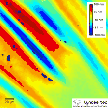
Non-scanning technologies as digital holographic microscopy enable 3D topography measurement in real-time. 3D topography is measured from a single camera acquisition as a consequence the acquisition rate is only limited by the camera acquisition rate, some systems measure topography at a frame rate of 1000 fps. Time-resolved systems enable measurement of topography changes as healing of smart materials or measurement of moving specimens. Time-resolved profilometers can be combined with a stroboscopic unit to measure MEMS vibrations in the MHz range. The stroboscopic unit provides excitation signal to the MEMS and provides trigger signal to light source and camera.
Advantage of time-resolved profilometers
- Robust against vibrations : unlike scanning methods, time-resolved profilometers acquisition time is in the milliseconds range
- No need of vertical calibration : vertical measurement does not depend on a scanning mechanism, digital holographic microscopy vertical measurement has an intrasinc vertical calibration based on laser source wavelength
- Sample are no longer static : response of specimen topography to external stimulus
- On-flight measurement : topography of moving sample is acquired thanks to short exposure time
- MEMS vibrations measurement : when systems are combined with a stroboscopic unit
Fiber-based optical profilometers
Fiber-based optical profilometers scan surfaces with optical probes which send light interference signals back to the profilometer detector via an optical fiber. Fiber-based probes can be physically located hundreds of meters away from the detector enclosure, without signal degradation. Here are the additional advantages of using fiber-based optical profilometers:
- Flexibility: Thanks to the small diameter of certain probes, surfaces can be scanned even inside hard-to-reach spaces, such as narrow crevices or small-diameter tubes.[6]
- Long profile acquisition: Since these probes generally acquire one point at a time and at very high sample speeds, acquisition of long (continuous) surface profiles is possible.
- Ruggedness: Scanning can take place in hostile environments, including very hot or cryogenic temperatures, or in radioactive chambers, while the detector is located at a distance, in a human-safe environment.[7]
- Ease of incorporating into industrial processes: fiber-based probes are easily installed in-process, such as above moving webs or mounted onto a variety of positioning systems.
See also
References
- 1 2 Jean M. Bennett, Lars Mattsson, Introduction to Surface Roughness and Scattering, Optical Society of America, Washington, D.C.
- 1 2 W J Walecki, F Szondy and M M Hilali, "Fast in-line surface topography metrology enabling stress calculation for solar cell manufacturing for throughput in excess of 2000 wafers per hour" 2008 Meas. Sci. Technol. 19 025302 (6pp) doi:10.1088/0957-0233/19/2/025302
- ↑ Nanoradian Probe
- ↑ Stout, K. J.; Blunt, Liam (2000). Three-Dimensional Surface Topography (2nd ed.). Penton Press. p. 22. ISBN 978-1-85718-026-8.
- ↑ Binnig, Gerd, Calvin F Quate, and Ch Gerber. ""Atomic force microscope." Physical review letters 56.9 (1986): 930".
- ↑ Dufour, Marc; Lamouche, G.; Gauthier, B.; Padioleau, C.; Monchalin, J.P. (2006). "Inspection of hard-to-reach industrial parts using small diameter probes" (PDF). SPIE - The International Society for Optical Engineering. doi:10.1117/2.1200610.0467. Retrieved December 15, 2010.
- ↑ Dufour, M. L.; Lamouche, G.; Detalle, V.; Gauthier, B.; Sammut, P. (April 2005). "Low-Coherence Interferometry, an Advanced Technique for Optical Metrology in Industry". Insight - Non-Destructive Testing and Condition Monitoring. 47 (4): 216–219. doi:10.1784/insi.47.4.216.63149. ISSN 1354-2575.
External links
| Wikimedia Commons has media related to Profilometers. |
- The Little Book of Profiling, the University of Michigan about road profiling