OmniVision Technologies
|
| |
| Private | |
| Traded as | NASDAQ: OVTI |
| Industry | Semiconductors |
| Founded | 1990 |
| Founder | Aucera Technology (Taiwan). |
| Headquarters | Santa Clara, California, U.S. |
Area served | Worldwide |
Key people | Lin shyue jenq |
| Products | Image sensor technologies |
| Revenue | $1.379B |
Number of employees | 2200 (2015) [1] |
| Website | www.ovt.com |
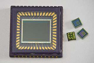
OmniVision Technologies Inc. is a corporation that designs and develops advanced digital imaging technologies and products for use in mobile phones, notebooks, netbooks and webcams, security and surveillance cameras, entertainment, digital still and video cameras, automotive and medical imaging systems. Headquartered in Santa Clara, California, OmniVision Technologies has offices in the USA, Western Europe and Asia, including a design center and testing facility in Shanghai, China.[2]
History
OmniVision was founded in 1995 by Aucera Technology (奧斯來科技, Taiwan).
Some company milestones:
- 2000: IPO
- 2002: First mobile handset camera accessory
- 2004: First 1.3-megapixel and 2-megapixel sensors for mobile phones
- 2005: Acquired CDM-Optics, a company founded to commercialize wavefront coding.[3]
- 2006: Introduced the world’s smallest NTS camera
- 2007: Launched first automotive HDR-SOC sensor
- 2008: Launched OmniBSI architecture
- 2011: Acquired Kodak patents [4]
- 2013: Launched PureCel CMOS image sensors
- 2015: Signed an agreement to be acquired by a group of Chinese investors, including Hua Capital Management, CITIC Capital Holdings and GoldStone Investment, for about $1.9 billion in cash in April 2015.[5]
Technologies
OmniPixel3-HS
OmniVision’s front-side illumination (FSI) technology architecture enhances image capture under very low lighting conditions. It is used to manufacture compact cameras in mobile handsets, notebook computers and other applications that require low-light performance without the need for flash.
OmniPixel3-HS is the technology behind its image sensor module that will, for example, be used by Dahua, a video surveillances provider, to produce cloud-based cameras for smart home systems.[6]
OmniBSI
Backside illuminated image (BSI) technology differs from FSI architectures in how light is delivered to the photosensitive area of the sensor. In FSI architectures, the light must first pass through transistors, dieletric layers, and metal circuitry. In contrast, OmniBSI technology turns the image sensor upside down and applies color filters and micro lenses to the backside of the pixels, resulting in light collection through the backside of the sensor. This puts the metal and dielectric layers below the sensor array, providing the most direct path for light to travel into the pixel, which optimizes image quality.
OmniBSI-2
The second-generation BSI technology, developed in cooperation with Taiwan Semiconductor Manufacturing Company Limited (TSMC), is built using custom 65 nm design rules and 300mm copper processes. This combination supports improved low-light sensitivity, dark current, and full-well capacity over the first-generation of BSI technology, as well as sharper image quality.
CameraCubeChip
In this camera module, sensor and lens manufacturing processes are combined using semiconductor stacking methodology. Wafer-level optical elements are fabricated in a single step by combining CMOS image sensors, chip scale packaging processes, (CSP) and wafer-level optics (WLO). These fully integrated chip products have camera functionality and are intended to produce thin, compact devices with advanced imaging capability.
PureCel
OmniVision developed its PureCel image sensor technology to provide added camera functionality to smartphones and action cameras. The technical goal was to provide smaller camera modules that enable larger optical formats and offer improved image quality, especially in low-light conditions.[7]
Both of these technologies are offered in a stacked die format (PureCel-S and PureCelPlus-S). This stacked die methodology separates the imaging array from the image sensor processing pipeline into a stacked die structure, allowing for additional functionality to be implemented on the sensor while providing for much smaller die sizes compared to non-stacked sensors. Unique to PureCelPlus-S are partial deep trench isolation (B-DTI) structures comprising an interfacial oxide, first deposited HfO, TaO, oxide, Ti-based liner, and a W core. This is OmniVision's first DTI structure, and the first metal filled B-DTI trench since 2013.[8]
Nyxel
Developed to address the low-light and night-vision performance requirements of advanced machine vision, surveillance, and automotive camera applications, OmniVision’s Nyxel near-infrared (NIR) imaging technology combines thick-silicon pixel architectures and careful management of the wafer surface texture to improve quantum efficiency (QE). In addition, extended deep trench isolation helps retain modulation transfer function without affecting the sensor’s dark current, further improving night vision capabilities. Unlike conventional NIR approaches, OmniVision’s Nyxel technology achieves 3x QE improvement for 850nm sensitivity and a 5x QE improvement for 940nm sensitivity[9]. Performance improvements include image quality, extended image-detection range and a reduced light-source requirement, leading to overall lower system power consumption[10].
References
- ↑ "Corporate Fact Sheet" (PDF). 2014. Retrieved 24 September 2015.
- ↑ "OmniVision Locations". Retrieved 13 September 2010.
- ↑ Michael R. Tomkins (28 March 2005). "OmniVision acquires CDM Optics". The Imaging Resource. Retrieved 25 September 2010.
- ↑ Vladimir Koifman, Image Sensor World “OmniVision Acquires 850 Kodak Patents for $65M” April 11. Retrieved November 15, 2015
- ↑ "OmniVision to Be Bought by Chinese Investors in $1.9 Billion Deal". re/code. 1 May 2015. Retrieved 4 May 2015.
- ↑ Lin, Melody. "Dahua Partners with OmniVision to Enable The Cloud-based HD Camera". SM Home. Retrieved 4 April 2016.
- ↑ Triggs, Rob. "Who's Who in the smartphone camera business". Android Authority. Retrieved 4 April 2016.
- ↑ Fontaine, Ray. "A Survey of Enabling Technologies in Successful Consumer Digital Imaging Products (Part 3: Pixel Isolation Structures)". TechInsights. Retrieved July 4, 2017.
- ↑ Carroll, James. "Nyxel near infrared technology from OmniVision offers increased quantum efficiency". Vision Systems Design. Retrieved October 9, 2017.
- ↑ Dirjish, Matthew. "Near-Infrared Technology Clears Up Night Vision Apps". Sensors Online. SeQuestex LLC. Retrieved October 9, 2017.