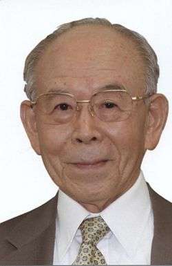
Isamu Akasaki
| Isamu Akasaki | |
|---|---|
 Isamu Akasaki | |
| Native name | 赤崎 勇 |
| Born |
January 30, 1929 Chiran, Kawanabe District, Kagoshima Prefecture |
| Nationality | Japanese |
| Alma mater |
Kyoto University Nagoya University |
| Awards |
Asahi Prize (2001) Takeda Award (2002) IEEE Edison Medal (2011) Nobel Prize in Physics (2014) Charles Stark Draper Prize (2015) |
| Scientific career | |
| Fields | Physics |
| Institutions |
Meijo University Nagoya University |
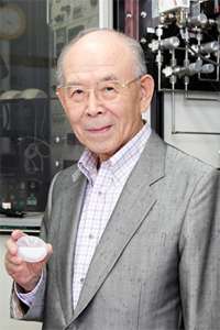
Isamu Akasaki (赤崎 勇 Akasaki Isamu, born January 30, 1929) is a Japanese physicist, specializing in the field of semiconductor technology and Nobel Prize laureate, best known for inventing the bright gallium nitride (GaN) p-n junction blue LED in 1989 and subsequently the high-brightness GaN blue LED as well.[1][2][3][4][5]
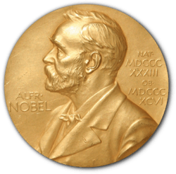
For this and other achievements Isamu Akasaki was awarded the Kyoto Prize in Advanced Technology in 2009[6] and the IEEE Edison Medal in 2011.[7] He was also awarded the 2014 Nobel prize in Physics, together with Hiroshi Amano and Shuji Nakamura,[8] "for the invention of efficient blue light-emitting diodes, which has enabled bright and energy-saving white light sources".
Early life and education
Born in Kagoshima Prefecture, Akasaki graduated from Kyoto University in 1952, and obtained a Dr.Eng. degree in Electronics from Nagoya University in 1964. During college years, he visited shrines and temples that local residents rarely visit, walked around the mountains of Shinshu during the summer vacation, enjoyed classes and enjoyed a fulfilling student era.[9]
Research
He started working on GaN-based blue LEDs in the late 1960s. Step by step, he improved the quality of GaN crystals and device structures[10] at Matsushita Research Institute Tokyo, Inc. (MRIT), where he decided to adopt metalorganic vapor phase epitaxy (MOVPE) as the preferred growth method for GaN.
In 1981 he started afresh the growth of GaN by MOVPE at Nagoya University, and in 1985 he and his group succeeded in growing high-quality GaN on sapphire substrate by pioneering the low-temperature (LT) buffer layer technology.[11][12]
This high-quality GaN enabled them to discover p-type GaN by doping with magnesium (Mg) and subsequent activation by electron irradiation (1989), to produce the first GaN p-n junction blue/UV LED (1989), and to achieve conductivity control of n-type GaN (1990)[13] and related alloys (1991)[14] by doping with silicon (Si), enabling the use of hetero structures and multiple quantum wells in the design and structure of more efficient p-n junction light emitting structures.
They achieved stimulated emission from the GaN firstly at room temperature in 1990,[15] and developed in 1995 the stimulated emission at 388 nm with pulsed current injection from high-quality AlGaN/GaN/GaInN quantum well device.[16] They verified quantum size effect (1991)[17] and quantum confined Stark effect (1997)[18] in nitride system, and in 2000 showed theoretically the orientation dependence of piezoelectric field and the existence of non-/semi-polar GaN crystals,[19] which have triggered today’s worldwide efforts to grow those crystals for application to more efficient light emitters.
Nagoya University Akasaki Institute
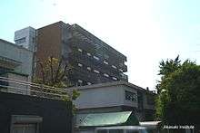
Professor Akasaki’s patents were produced from these inventions, and the patents have been rewarded as royalties. Nagoya University Akasaki Institute[20] opened on October 20, 2006. The cost of construction of the institute was covered with the patent royalty income to the university, which was also used for a wide range of activities in Nagoya University. The institute consists of an LED gallery to display the history of blue LED research/developments and applications, an office for research collaboration, laboratories for innovative research, and Professor Akasaki's office on the top sixth floor. The institute is situated in the center of the collaboration research zone in Nagoya University Higashiyama campus.
Professional record
Mr. Akasaki started as a Research Scientist in 1952 and until 1959 at Kobe Kogyo Corporation (now, Fujitsu Ltd.). In 1959 he was a Research Associate, Assistant Professor, and Associate Professor at the Department of Electronics at Nagoya University until 1964. Later in 1964, he was the Head of Basic Research Laboratory at Matsushita Research Institute Tokyo, Inc. until 1974 to later become a General Manager of Semiconductor Department (in the same institute until 1981. In 1981 he became a Professor in the Department of Electronics at Nagoya University until 1992.
It is worth to mention that from 1987 to 1990 he was a Project Leader of "Research and Development of GaN-based Blue Light–Emitting Diode" sponsored by Japan Science and Technology Agency(JST). Then from 1993 as a Project Leader of "Research and Development of GaN-based Short-Wavelength Semiconductor Laser Diode" sponsored by JST until 1999. While he was working as a Project Leader of "Research and Development of GaN-based Short-Wavelength Semiconductor Laser Diode," he started in 1995 and until 1996 as a Visiting Professor of the Research Center for Interface Quantum Electronics at Hokkaido University. In 1996 he was a Project Leader of the Japan Society for the Promotion of Science(JSPS)’s "Research for the Future" program" up to 2001. From 1996 he started as a Project Leader of "High-Tech Research Center for Nitride Semiconductors" at Meijo University, sponsored by MEXT until 2004. From 2003 up to 2006 he was the Chairman of "R&D Strategic Committee on the Wireless Devices Based on Nitride Semiconductors" sponsored by METI.
He is still working as a Professor Emeritus of Nagoya University, Professor of Meijo University since 1992. Also, as a Director of Research Center for Nitride Semiconductors at Meijo University since 2004. Also, still working as a Research Fellow at Akasaki Research Center of Nagoya University since 2001.
Honors and awards
Scientific and academic
- 1989 – Japanese Association for Crystal Growth (JACG) Award
- 1991 – Chu-Nichi Culture Prize[21]
- 1994 – Technological Contribution Award, Japanese Association for Crystal Growth in commemoration of its 20th anniversary
- 1995 – Heinrich Welker Gold Medal, the International Symposium on Compound Semiconductors
- 1996 – Engineering Achievement Award, the Institute of Electrical and Electronics Engineers / Lasers Electro-Optics Society
- 1998 – Inoue Harushige Award, Japan Science and Technology Agency
- 1998 – C&C Prize, the Nippon Electric Company Corporation[22]
- 1998 – Laudise Prize, the International Organization for Crystal Growth[23]
- 1998 – Jack A. Morton Award, the Institute of Electrical and Electronics Engineers[24]
- 1998 – Rank Prize, the Rank Prize Foundation[25]
- 1999 – Fellow, the Institute of Electrical and Electronics Engineers[26]
- 1999 – Gordon E. Moore Medal for Outstanding Achievement in Solid State Science and Technology, the Electrochemical Society[27]
- 1999 – Honoris Causa Doctorate, the University of Montpellier II
- 1999 – Toray Science and Technology Prize, Toray Science Foundation[28]
- 2001 – Asahi Prize, the Asahi Shinbun Cultural Foundation[29]
- 2001 – Honoris Causa Doctorate, Linkoping University
- 2002 – Outstanding Achievement Award, the Japan Society of Applied Physics
- 2002 – Fujihara Award, the Fujihara Foundation of Science[30]
- 2002 – Takeda Award, the Takeda Foundation[31]
- 2003 – President's Award, the Science Council of Japan (SCJ)[32]
- 2003 – Solid State Devices & Materials (SSDM) Award
- 2004 – Tokai TV Culture Prize
- 2004 – University Professor, Nagoya University
- 2006 – John Bardeen Award, the Minerals, Metals & Materials Society[33]
- 2006 – Outstanding Achievement Award, the Japanese Association for Crystal Growth
- 2007 – Honorable Lifetime Achievement Award, the 162nd Research Committee on Wide Bandgap Semiconductor Photonic and Electronic Devices, Japan Society for the Promotion of Science (JSPS)
- 2008 – Foreign Associate, the US National Academy of Engineering[34]
- 2009 – Kyoto Prize Advanced Technology, the Inamori Foundation[35]
- 2010 – Lifetime Professor, Meijo University
- 2011 – Edison Medal, the Institute of Electrical and Electronics Engineers[7]
- 2011 – Special Award for Intellectual Property Activities, the Japan Science and Technology Agency
- 2011 – Minami-Nippon Culture Prize-Honorable Prize
- 2014 – Nobel Prize in Physics together with prof. Hiroshi Amano and prof. Shuji Nakamura[8]
- 2015 – Charles Stark Draper Prize
National
- 1997 – Medal with Purple Ribbon, the Japanese Government[36]
- 2002 – Order of the Rising Sun, Gold Rays with Neck Ribbon, the Japanese Government[37]
- 2004 – Person of Cultural Merit, the Japanese Government
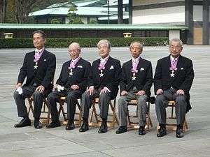
- 2011 – Order of Culture, the Japanese Emperor[38][39][40]
See also
References
- ↑ "Japanese Journal of Applied Physics". Jsap.jp. Retrieved 2015-11-10.
- ↑ "Japanese Journal of Applied Physics". jsap.jp. Retrieved 2015-11-10.
- ↑ Hiroshi Amano, Masahiro Kito, Kazumasa Hiramatsu and Isamu Akasaki: "P-Type Conduction in Mg-doped GaN Treated with Low-Energy Electron Beam Irradiation (LEEBI)", Jpn. J. Appl. Phys. Vol. 28, No.12, December 1989, pp. L2112-L2114, (accepted for pub. Nov. 1989).
- ↑ I. Akasaki, H. Amano, M. Kito and K. Hiramatsu :"Photoluminescence of Mg doped p-type GaN and electroluminescence of GaN p-n junction LED" J. Cryst. Growth, Vol. 48&49 pp.666-670, 1991
- ↑ Isamu Akasaki, Hiroshi Amano, Kenji Itoh, Norikatsu Koide and Katsuhide Manabe: "GaN-based UV/blue light emitting devices", Inst. Phys. Conf. Ser. No.129, pp. 851-856, 1992
- ↑ "INAMORI FOUNDATION". Inamori-f.or.jp. Archived from the original on March 4, 2016. Retrieved November 10, 2015.
- 1 2 "IEEE Jack S. Kilby Signal Processing Medal Recipients" (PDF). IEEE. Retrieved April 15, 2012.
- 1 2 "The 2014 Nobel Prize in Physics - Press Release". Nobelprize.org. Nobel Media AB 2014. Retrieved October 7, 2014.
- ↑ http://www.kyoto-u.ac.jp/ja/about/history/honor/award_b/nobel/2015/akasaki/interview.html ノーベル物理学賞受賞者・赤﨑勇博士と京都大学 -大学時代に育まれた研究者の芽-
- ↑ Y. Ohki, Y. Toyoda, H. Kobayasi and I. Akasaki: "Fabrication and properties of a practical blue-emitting GaN m-i-s diode. Inst. Phys. Conf. Ser. No. 63, pp. 479-484 (Proc. of the 9th Intl. Symposium on Gallium Arsenide and Related Compounds, 1981).
- ↑ H. Amano, N. Sawaki I. Akasaki and Y. Toyoda: "Metalorganic vapor phase epitaxial growth of a high quality GaN film using an AlN buffer layer,"
- ↑ Isamu Akasaki, Hiroshi Amano, Yasuo Koide, Kazumasa Hiramatsu and Nobuhiko Sawaki: "Effects of AlN buffer layer on crystallographic structure and on electrical and optical properties of GaN and Ga1-xAl xN (0<x < = 0,4) films grown on sapphire substrate by MOVPE", J. Crystal Growth, Vol.98 (1989), pp.209-219
- ↑ H. Amano and I. Akasaki: "Fabrication and Properties of GaN p-n Junction LED", Mater. Res. Soc. Extended Abstract (EA-21), pp.165-168, 1990, (Fall Meeting 1989)
- ↑ Hiroshi Murakami, Tsunemori Asahi, Hiroshi Amano, Kazumasa Hiramatsu, Nobuhiko Sawaki and Isamu Akasaki: "Growth of Si-doped AlxGa 1-xN on (0001) sapphire substrate by metalorganic vapor phase epitaxy", J. Crystal Growth, Vol.115 (1991), pp. 648-651.
- ↑ H. Amano, T. Asahi and I. Akasaki: "Stimulated Emission Near Ultraviolet at Room Temperature from a GaN Film Grown on Sapphire by MOVPE Using an AlN Buffer Layer" Jpn. J. Appl. Phys. Vol. 29, pp. L205-L206, 1990.
- ↑ Isamu Akasaki, Hiroshi Amano, Shigetoshi Sota, Hiromitsu Sakai, Toshiyuki Tanaka and Masayoshi Koike: "Stimulated Emission by Current Injection from an AlGaN/GaN/GaInN Quantum Well Device" Jpn. J. Appl. Phys., Vol. 34 (1995) pp. L1517-1519, Part 2, No.11B, 15 November 1995 (accepted for pub. October 16, 1995).
- ↑ K. Itoh, T. Kawamoto, H. Amano, K. Hiramatsu and I. Akasaki: "Metalorganic Vapor Phase Epitaxial Growth and Properties of GaN/Al0.1Ga0.9N Layered Structures" Jpn. J. Appl. Phys. Vol. 30, pp.1924-1927, 1991.
- ↑ T. Takeuchi, S. Sota, M. Katsuragawa, M. Komori, H. Takeuchi, H. Amano and I. Akasaki: "Quantum-Confined Stark Effect due to Piezoelectric Fields in GaInN Strained Quantum Wells" Jpn. J. Appl. Phys., Vol.36, Pt. 2, No. 4A, pp. L382-385, 1997.
- ↑ Tetsuya Takeuchi, Hiroshi Amano and Isamu Akasaki: "Theoretical Study of Orientation Dependence of Piezoelectric Effects in Wurtzite Strained GaInN/GaN Heterostructures and Quantum Wells", Jpn. J. Appl. Phys. Vol. 39, pp. 413-416, Part1, No.2A, Feb.2000. (accepted for pub., November 1, 1999).
- ↑ Archived October 17, 2012, at the Wayback Machine.
- ↑ "中日文化賞". 中日新聞 CHUNICHI Web.
- ↑ "NEC: News Release 98/11/04-01". Nec.co.jp. Retrieved 2015-11-10.
- ↑ "International Organization for Crystal Growth". Iocg.org. Retrieved 2015-11-10.
- ↑ (PDF) https://web.archive.org/web/20141013182218/http://www.ieee.org/documents/morton_rl.pdf. Archived from the original (PDF) on October 13, 2014. Retrieved January 7, 2014. Missing or empty
|title=(help) - ↑ Archived December 13, 2012, at the Wayback Machine.
- ↑ https://web.archive.org/web/20121226163602/http://www.ieee.org/membership_services/membership/fellows/chronology/fellows_1999.html. Archived from the original on December 26, 2012. Retrieved February 23, 2013. Missing or empty
|title=(help) - ↑ "ECS SSS&T Award". Electrochem.org. Retrieved 2015-11-10.
- ↑ "Toray Science and Technology Prize : List of Winners". Toray.com. Retrieved 2015-11-10.
- ↑ The Asahi Shimbun Company. "The Asahi Shimbun Company - The Asahi Prize - English Information". Asahi.com. Retrieved 2015-11-10.
- ↑ "Archived copy". Archived from the original on April 11, 2013. Retrieved March 1, 2013.
- ↑ "Social/Economic Well-Being : Technical Achievement: The Development of Blue Light Emitting Semiconductor Devices - Development of the blue light emitting diode and laser diode is the final link in completing the light spectrum for semiconductor devices". Takeda-foundation.jp. Retrieved 2015-11-10.
- ↑ "IAP - About IAP". Interacademies.net. Retrieved 2015-11-10.
- ↑ "Recipient: 2006 John Bardeen Award". Tms.org. Archived from the original on March 4, 2016. Retrieved November 10, 2015.
- ↑ "NAE Website - Dr. Isamu Akasaki". Nae.edu. Retrieved 2015-11-10.
- ↑ "INAMORI FOUNDATION". Inamori-f.or.jp. Archived from the original on March 4, 2016. Retrieved November 10, 2015.
- ↑ "Types of Medals". cao.go.jp.
- ↑ "Orders of the Rising Sun". Cao.go.jp. Retrieved 2015-11-10.
- ↑ "Order of Culture". Cao.go.jp. Retrieved 2015-11-10.
- ↑ "Archived copy". Archived from the original on April 11, 2013. Retrieved March 1, 2013.
- ↑ "M͎͎". Nifty.com. Archived from the original on September 13, 2016. Retrieved November 10, 2015.
Further reading
- Insights & Enterprise in PHOTONICS SPECTRA, 54, November 2004
- Materials Research Society Symposium Proceedings, Volume 639 (2000), pages xxiii-xxv
External links
2014 Nobel Prize laureates | ||
|---|---|---|
| Chemistry |
|  |
| Literature | Patrick Modiano (France) | |
| Peace |
| |
| Physics |
| |
| Physiology or Medicine |
| |
| Economic Sciences | Jean Tirole (France) | |
| ||
| Chemistry |
| |
|---|---|---|
| Literature |
| |
| Peace |
| |
| Physics |
| |
| Physiology or Medicine |
| |
| Authority control |
|---|