Indium arsenide
 | |
 | |
| Names | |
|---|---|
| IUPAC name
Indium(III) arsenide | |
| Other names
Indium monoarsenide | |
| Identifiers | |
3D model (JSmol) |
|
| ChemSpider | |
| ECHA InfoCard | 100.013.742 |
PubChem CID |
|
| |
| |
| Properties | |
| InAs | |
| Molar mass | 189.740 g/mol |
| Density | 5.67 g/cm3 |
| Melting point | 942 °C (1,728 °F; 1,215 K) |
| Band gap | 0.354 eV (300 K) |
| Electron mobility | 40000 cm2/(V*s) |
| Thermal conductivity | 0.27 W/(cm*K) (300 K) |
Refractive index (nD) |
3.51 |
| Structure | |
| Zinc Blende | |
a = 6.0583 Å | |
| Thermochemistry | |
Heat capacity (C) |
47.8 J·mol−1·K−1 |
Std molar entropy (S |
75.7 J·mol−1·K−1 |
Std enthalpy of formation (ΔfH |
-58.6 kJ·mol−1 |
| Hazards | |
| Safety data sheet | External SDS |
| GHS pictograms |   |
| GHS signal word | Danger[2] |
| H301, H331[2] | |
| P261, P301+310, P304+340, P311, P405, P501[2] | |
| NFPA 704 | |
| Related compounds | |
Other anions |
Indium phosphide Indium antimonide |
Other cations |
Gallium arsenide |
Except where otherwise noted, data are given for materials in their standard state (at 25 °C [77 °F], 100 kPa). | |
| Infobox references | |

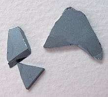
Indium arsenide, InAs, or indium monoarsenide, is a semiconductor composed of indium and arsenic. It has the appearance of grey cubic crystals with a melting point of 942 °C.[3]
Indium arsenide is used for construction of infrared detectors, for the wavelength range of 1–3.8 µm. The detectors are usually photovoltaic photodiodes. Cryogenically cooled detectors have lower noise, but InAs detectors can be used in higher-power applications at room temperature as well. Indium arsenide is also used for making of diode lasers.
Indium arsenide is similar to gallium arsenide and is a direct bandgap material.
Indium arsenide is sometimes used together with indium phosphide. Alloyed with gallium arsenide it forms indium gallium arsenide - a material with band gap dependent on In/Ga ratio, a method principally similar to alloying indium nitride with gallium nitride to yield indium gallium nitride.
InAs is well known for its high electron mobility and narrow energy bandgap. It is widely used as terahertz radiation source as it is a strong photo-Dember emitter.
Quantum dots can be formed in a monolayer of indium arsenide on indium phosphide or gallium arsenide. The mismatches of lattice constants of the materials create tensions in the surface layer, which in turn leads to formation of the quantum dots.[4] Quantum dots can also be formed in indium gallium arsenide, as indium arsenide dots sitting in the gallium arsenide matrix.
References
- ↑ Lide, David R. (1998), Handbook of Chemistry and Physics (87 ed.), Boca Raton, FL: CRC Press, pp. 4–61, ISBN 0-8493-0594-2
- 1 2 3 4 "Indium Arsenide". American Elements. Retrieved October 12, 2018.
- ↑ "Thermal properties of Indium Arsenide (InAs)". Retrieved 2011-11-22.
- ↑ "oe magazine - eye on technology". Archived from the original on 2006-10-18. Retrieved 2011-11-22.
External links
- Ioffe institute data archive entry
- National Compound Semiconductor Roadmap entry for InAs at ONR web site
| Basic types |
|
|---|---|
| Hybrid types |
|
| Other Types | |
| Theory | |
| Materials |
|