WDC 65C02
The Western Design Center (WDC) 65C02 microprocessor is an enhanced CMOS version of the popular NMOS-based 8-bit MOS Technology 6502 microprocessor—the CMOS redesign being made by Bill Mensch in 1978. Over various periods of time, the 65C02 has been second-sourced by NCR, GTE, Rockwell, Synertek and Sanyo. The 65C02 has been used in some home computers, as well as in embedded applications, including medical-grade implanted devices.
Introduction and features
The 65C02 is a low cost, general-purpose 8-bit microprocessor (8-bit registers and data bus) with a 16-bit program counter and address bus. The variable length instruction set and manually optimized core size are intended to make the 65C02 well suited for low power system-on-chip (SoC) designs.
A Verilog hardware description model is available for designing the W65C02S core into an application-specific integrated circuit (ASIC) or a field-programmable gate array (FPGA). As is common in the semiconductor industry, WDC offers a development system, which includes a developer board, an in-circuit emulator (ICE) and a software development system.
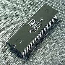
The W65C02S–14 is the production version of the 65C02 microprocessor, and is available in PDIP, PLCC and QFP packages through distribution. The maximum officially supported ϕ2 (primary) clock speed is 14 MHz, indicated by the –14 part number suffix. The "S" designation indicates that the part has a fully static core, a feature that allows ϕ2 to be slowed down or fully stopped in either the high or low state with no loss of data. Typical microprocessors not implemented in CMOS have dynamic cores and will lose their internal register contents (and thus crash) if they are not continuously clocked at a rate between some minimum and maximum specified values.
| 65C02 registers | |||||||||||||||||||||||||||||||||||||||||||||||||||||||||||||||||||||||||||||||||||||||||||||||||||||||||||||||||||||||||||||||||||||||||||||||||||||||||||||||||||||||||||||||||||||||||||
| |||||||||||||||||||||||||||||||||||||||||||||||||||||||||||||||||||||||||||||||||||||||||||||||||||||||||||||||||||||||||||||||||||||||||||||||||||||||||||||||||||||||||||||||||||||||||||
General logic features
- 8-bit data bus
- 16-bit address bus (providing an address space of 64 K bytes)
- 8-bit arithmetic logic unit (ALU)
- 8-bit processor registers:
- 16-bit program counter
- 69 instructions, implemented by 212 operation codes
- 16 addressing modes, including zero page addressing
Logic features
- Vector pull (VPB) output indicates when interrupt vectors are being addressed
- Memory lock (MLB) output indicates to other bus masters when a read-modify-write instruction is being processed
- WAit-for-Interrupt (WAI) and SToP (STP) instructions reduce power consumption, decrease interrupt latency and enable synchronization with external events
Electrical features
- Supply voltage specified at 1.71 V to 5.25 V
- Current consumption (core) of 0.15 and 1.5 mA per MHz at 1.89 V and 5.25 V respectively
- Variable length instruction set, enabling code size optimization over fixed length instruction set processors, results in power savings
- Fully static circuitry allows stopping the clock to conserve power
Clocking features
The W65C02S may be operated at any convenient supply voltage (VDD) between 1.8 and 5 volts (±5%). The data sheet AC characteristics table lists operational characteristics at 5 V at 14 MHz, 3.3 V or 3 V at 8 MHz, 2.5 V at 4 MHz, and 1.8 V at 2 MHz. This information may be an artifact of an earlier data sheet, as a graph indicates that typical devices are capable of operation at higher speeds than suggested by the AC characteristics table, and that reliable operation at 20 MHz should be readily attainable with VDD at 5 volts, assuming the supporting hardware will allow it.
The W65C02S may also be operated at non-integral clock rates such as 13.5 MHz (digital SDTV luma sampling rate), 14.31818 MHz (NTSC colour carrier frequency × 4), 14.75 MHz (PAL square pixels), 14.7456 (baud rate crystal), etc., as long as VDD is sufficient to support the frequency. Designer Bill Mensch has pointed out that FMAX is affected by off-chip factors, such as the capacitive load on the microprocessor's pins. Minimizing load by using short signal tracks and fewest devices helps raise FMAX. The PLCC and QFP packages have less pin-to-pin capacitance than the PDIP package, and are more economical in the use of printed circuit board space.
WDC has reported that FPGA realizations of the W65C02S have been successfully operated at 200 MHz.
Comparison with the NMOS 6502
Instruction set
The 65C02 shares its predecessor's 8-bit instruction set architecture and 16-bit memory address space $0000 to $FFFF allowing access to a total memory map of 64K. "Zero Page" spans $0000 to $00FF. "Page 1" spans memory address space $0100 to $01FF and is dedicated for the stack. On this processor the stack grows downwards with the stack pointer starting at $01FF and decrementing as the stack grows.
The 65C02 adds a number of improvements and documented opcodes, the most useful being instructions that can push or pull the X and Y index registers to/from the stack. Undefined opcodes have been converted into NOPs, although of varying instruction lengths.
Significantly, the defective "indirect jump page wrap" instruction (JMP (<ADDR>), where <ADDR> straddles a memory page boundary) has been fixed, eliminating a source of trouble for unwary assembly language programmers. This instruction has also been enhanced with .X register indexing, making it possible to code JMP (<ADDR>,X), enabling the development of a simple jump table management methodology.
Some variants of the 65C02 (including the WDC W65C02S and the Rockwell R65C00 family) feature individual bit manipulation operations (RMB, SMB, BBR and BBS). The 65SC02 was also available, which lacked these operations.
Status register
Other problems with the 6502, fixed in the 65C02, relate to its program status register, which contains eight system flags. Some flags are set or reset under program control. Others reflect the status of the machine after arithmetic or bit manipulation instructions.
6502 status flags, with meanings when set:
| N | — | Negative result |
| V | — | Sign bit overflow |
| 1 | — | Undefined (always set) |
| B | — | Break flag (set by BRK and PHP instructions) |
| D | — | Decimal mode enabled |
| I | — | IRQ disabled |
| Z | — | Zero result |
| C | — | Arithmetic carry (borrow) |
In all NMOS logic forms of the 6502, the decimal flag (D flag) is not initialized to a known state following reset (state is "random") or when an interrupt is processed (state has been kept from "before the interrupt occurred"), which may lead to arbitrary behavior. This forces 6502 programmers to use the CLD instruction early in the reset handler code (it is generally the second instruction executed after SEI), as well as in the front end of the interrupt handler. The 65C02 addresses these problems by causing the D flag to be cleared at reset or upon receipt of an interrupt (after the status register is pushed onto the stack).
Also, in NMOS 6502s, the N, V, and Z flags are invalid when the processor is operating in decimal mode. The 65C02 fixes this problem (at the cost of an additional clock cycle), and thus increases the usefulness of decimal mode. [1]
65SC02
The 65SC02 is a variant of the WDC 65C02 without bit instructions.[2] The WDC 65C02 is the base for the HuC6280 by NEC used in their video game console TG-16 (PC-Engine)[3]
Notable uses of the 65C02
Home computers
- Apple IIc portable by Apple Computer (NCR 1.023 MHz)
- Enhanced Apple IIe by Apple Computer (1.023 MHz)
- BBC Master home/educational computer, by Acorn Computers Ltd (2 MHz 65SC12 plus optional 4 MHz 65C102 second processor)
- Replica 1 by Briel Computers, a replica of the Apple I hobbyist computer (1 MHz)
- Laser 128 series clones of Apple II
- KIM-1 Modern Replica of the MOS/CBM KIM-1 by Briel Computing
Video game consoles
- Nintendo Entertainment System aka FAMICOM (RP2A07 1.66 MHz)
- Atari Lynx handheld (65SC02 @ ~4 MHz)
- NEC PC Engine aka TurboGrafx-16 (HuC6280 @ 7.16 MHz)
- GameKing handhelds (6 MHz) by Timetop
- Watara Supervision handhelds (65SC02 @ 4 MHz)
Other products
- TurboMaster accelerator cartridge for the Commodore 64 home computer (65C02 @ 4.09 MHz)
- many dedicated chess computers i.e.: Mephisto MMV, Novag Super Constellation, Fidelity Elite and many more (4–20 MHz)
See also
References
- ↑ "Differences between NMOS 6502 and CMOS 65c02". Retrieved 27 February 2018.
N, V, and Z flags were incorrect after decimal operation (but C was ok). (CMOS adds one cycle to fix them.)
- ↑ Rodnay Zaks, Programmierung des 6502. Jetzt auch mit 6510, 65C02, 65SC02, p. 348
- ↑ http://archaicpixels.com/HuC6280
External links
- W65C02S website - Western Design Center
- W65C02S datasheet - Western Design Center
- 65xx/65Cxx/65SCxx Differences - CPU World
- 6502/65C02/65C816 Instruction Set Decoded – From Neil Parker's Apple II page