Computer Architecture
2.1.1 Outline the architecture of the central processing unit (CPU) and the functions of the arithmetic logic unit (ALU) and the control unit (CU) and the registers within the CPU.
A major defining point in the history of computing was the realisation in 1944–1945 that data and instructions to manipulate data were logically the same and could be stored in the same place. The computer design built upon this principle, which became known as the von Neumann Architecture, is still the basis for computer today. Although the name honours John von Neumann, a brilliant mathematician who worked on the construction of the atomic bomb, the idea probably originated with J. Presper Echkert and John Mauchly, two other early pioneers who worked on the ENIAC at the Moore School at the University of Pennsylvania during the same time period.
von Neumann Architecture
Another major characteristic of the von Neumann architecture is that the units that process information are separate from the units that store information. This characteristic leads to the following components of the von Neumann architecture.
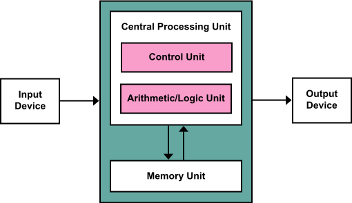
- The memory unit that holds both data and instructions.
- The arithmetic/logic gate unit that is capable of performing arithmetic and logic operations on data.
- The input unit that moves data from the outside world into the computer.
- The output unit that moves results from inside the computer to the outside world.
- The control unit that acts as the stage unit to ensure that all the other components act in concert.
Memory
Memory is a collection of cells, each with a unique physical address. We use the generic word cell here rather than byte, because the number of bits in each addressable location, called the memory's addressability, varies from one machine to another. Today, most computers are byte addressable.
To fully illustrate the concept of memory, take a computer with 4GB of RAM as an example. The memory consists of 4 × 230 bytes, which means each byte of the computer is uniquely addressable, and the addressability of the machine is 8 bits. The cells in memory are numbered consecutively beginning with 0. For example, if the addressability is 8, and there are 256 cells of memory, the cells would be addressed as follows:
| Address | Contents |
|---|---|
| 00000000 | 11100011 |
| 00000001 | 01010101 |
| 11111100 | 00000000 |
| 11111101 | 11111111 |
| 11111110 | 10101010 |
| 11111111 | 00110011 |

What are the contents of address 11111110? The bit pattern stored at that location is 10101010. However, what the contents actually represents, be it instructions, value, sign, etc. will be discussed later. What is important, however, is to understand that the bit pattern is information and can be interpreted.
When referring to the bits in a byte or word, the bits are numbered from right to left beginning with zero. The bits in address 1111110 are numbered as follows:
| Bit Position | 7 | 6 | 5 | 4 | 3 | 2 | 1 | 0 |
|---|---|---|---|---|---|---|---|---|
| Contents | 1 | 0 | 1 | 0 | 1 | 0 | 1 | 0 |
Arithmetic/Logic Unit
The Arithmetic/Logic Unit (ALU) is capable of performing basic arithmetic operations such as adding, subtracting, multiplying, and dividing two numbers. This unit is also capable of performing logical operations such as AND, OR, and NOT. The ALU operates on words, a natural unit of data associated with a particular computer design. Historically, the word length of a computer has been the number of bits processed at once by the ALU. However, the current Intel line of processors has blurred this definition by defining the word length to be 16 bits. The processor can work on words (of 16 bits), double words (32 bits), and quadwords (64 bits). In the rest of this wiki, when referring to word, it will be of the historical nature aforementioned.
Most modern ALUs have a small number of special storage units called Registers. These registers contain one word and are used to store information that is needed again immediately. For example, in the calculation of 1 × (2 + 3). 2 is first added to 3 and the result is multiplied by 1. Rather than storing the result of adding 2 and 3 in memory and then retrieving it to multiply it by 1, the result is left in a register and the contents of the register is multiplied by 1. Access to registers is much faster than access to memory locations.
Input/Output Units
All of the computing power in the world would not be useful if one could not input values into the calculations from the outside or report to the outside the results of said calculations. Input and output units are the channels through which the computer communicates with the outside world.
An Input Unit is a device through which data and programs from the outside world are entered into the computer. The first input units interpreted holes punched on paper tape or cards. Modern-day input devices, however, include, but are not limited to; keyboards, mice, cameras (also known as, simply, webcams), and scanning devices.
An Output Unit is a device through which results stored in the computer memory are made available to the outside world. Examples include printers and screen monitors.
Control Unit
The Control Unit is the organising force in the computer, for it is in charge of the Fetch-Execute Cycle. There are two special registers in the control unit. The Instruction Register (IR) contains the instruction that is being executed, and the Program Counter (PC) contains the address of the next instruction to be executed. Because the ALU and the control unit work so closely together they are often thought of as one unit called the Central Processing Unit (CPU).

Above is a simplified view of the flow of information through the parts of a von Neumann machine. The parts are connected to one another by a collection of wires called a bus, through which data travels in the computer. Each bus carries three kinds of information; address, data, and control. An address is used to select the memory location or device to which data will go, or from which it will be taken. Data then flows over the bus between CPU, memory, and I/O Devices. The control information is used to manage the flow of addresses and data. For example, a control signal will typically be used to determine the direction in which the data is flowing either to or from the CPU. The Bus Width is the number of bits that it can transfer simultaneously. The wider the bus, the more address or data bits it can move at once.
2.1.3 Explain the use of cache memory.
Because memory accesses are very time consuming relative to the speed of the processor, many architectures provide Cache Memory. Cache memory is a small amount of fast-access memory into which copies of frequently used data are stored. Before a main memory access is made, the CPU checks whether the data is stored in the cache memory. Pipelining is another technique used to speed up the Fetch-Execute Cycle. This technique splits an instruction into smaller steps that can be overlapped.
In a personal computer, the component in a von Neumann machine reside physically a printed circuit board called the Motherboard. The motherboard also has connections for attaching other devices to the bus, such as a mouse, a keyboard, or additional storage devices.
So what does it mean to say that a machine is an n-bit processor? The variable n usually refers to the number of bits in the CPU general registers: Two n-bit numbers can be added with a single instruction. It also can refer to the width of the bus, which is the size of the addressable memory—but not always. In addition, n can refer to the width of the data bus—but not always.
The Fetch-Execute Cycle
2.1.4 Explain the machine instruction cycle.
Before looking at how a computer does what it does, let us look at what it can do. The definition of a computer outlines its capabilities; a computer is an electronic device that can store, retrieve, and process data. Therefore, all of the instructions that we give to the computer relate to storing, retrieving, and processing data.
The underlying principle of the von Neumann machine is that data and instructions are stored in memory and treated alike. This means that instructions and data are both addressable. Instructions are stored in contiguous memory locations; data to be manipulated are stored together in a different part of memory. To start the Fetch-Execute Cycle,first of all the data is loaded to the main memory by the operating system, the address of the first instruction is placed onto the program counter.

The process cycle includes four steps:
- Fetch the next instruction,
- Decode the instruction
- Get data if needed,
- Execute the instruction.
Fetch the Next Instruction
The PC increments one by one to point to the next instruction to be executed, so the control unit goes to the address in the memory address register which holds the address of the next instruction specified in the PC, takes it to the main memory through the address bus and returns it to the memory buffer register via the data bus. The MBR is a two way register that temporarily holds data fetched from the Memory(cache or RAM), makes a copy of the contents, and places the copy in the IR. At this point the IR contains the instruction to be executed. Before going to the next step in the cycle, the PC must be updated to hold the address of the next instruction to be executed when the current instruction has been completed. There after the instruction register is responsible for the instruction to be solved by the CU. the CU checks on the status of the instruction and then allows execution. Because the instructions are stored contiguously in memory, adding the number of bytes in the current instruction to the PC should put the address of the next instruction into the PC. Thus the control unit increments the PC. It is possible that the PC may be changed later by the instruction being executed.
In the case of an instruction that must get additional data from memory, the ALU sends an address to the memory bus, and the memory responds by returning the value at that location. In some computers, data retrieved from memory may immediately participate in an arithmetic or logical operation. Other computers simply save the data returned by the memory into a register for processing by a subsequent instruction. At the end of execution, any result from the instruction may be saved either in registers or in memory.
Decode the Instruction
To execute the instruction in the instruction register, the control unit has to determine what instruction it is. It might be an instruction to access data from an input device, to send data to an output device, or to perform some operation on a data value. At this phase, the instruction is decoded into control signals. That is, the logic of the circuitry in the CPU determines which operation is to be executed. This step shows why a computer can execute only instructions that are expressed in its own machine language. The instructions themselves are literally built into the circuit.
Get Data If Needed
The instruction to be executed may potentially require additional memory accesses to complete its task. For example, if the instruction says to add the contents of a memory location to a register, the control unit must get the contents of the memory location.
Execute the Instruction
Once an instruction has been decoded and any operands (data) fetched, the control unit is ready to execute the instruction. Execution involves sending signals to the arithmetic/logic unit to carry out the processing. In the case of adding a number to a register, the operand is sent to the ALU and added to the contents of the register.
When the execution is complete, the cycle begins again. If the last instruction was to add a value to the contents of a register, the next instruction probably says to store the results into a place in memory. However, the next instruction might be a control instruction—that is, an instruction that asks a question about the result of the last instruction and perhaps changes the contents of the program counter.
Hardware has changed dramatically in the last half-century, yet the von Neumann model remains the basis of most computers today. As Alan Perlis, a well-known computer scientist once said;
Sometimes I think the only universal in the computing field is the Fetch-Execute Cycle.—Alan Perlis, 1981.
RAM and ROM
2.1.4 Describe primary memory.
RAM stands for Random-Access Memory. RAM is memory in which each cell (usually a byte) can be directly accessed. Inherent in the idea of being able to access each location is the ability to change the contents of each location. That is, storing something else into that place can change the bit pattern in each cell.
In addition to RAM, most computers contain a second kind of memory called ROM. ROM stands for Read-Only Memory. The contents in locations in ROM cannot be changed. Their contents are permanent and cannot be altered by a second operation. Placing the bit pattern in ROM is called burning. The bit pattern is burnt either at the time the ROM is manufactured or at the time the computer parts are assembled.
RAM and ROM are differentiated by a very basic property; RAM is volatile, and ROM is not. This means that RAM does not retain its bit configuration when the power is turned off, but ROM does. Because ROM is stable and cannot be changed, it is used to store the instructions that the computer needs to start itself. Frequently used software is also stored in ROM so that the system does not have to read the software each time the machine is turned on. Main memory usually contains some ROM along with the general-purpose RAM.
Secondary Storage Devices
2.1.5 Identify the need for persistent storage.
An input device is the means by which data and programs are entered into the computer and stored into memory. An output device is the means by which results are sent back to the user. Because most of main memory is volatile and limited, it is essential that there be other types of storage devices where programs and data can be stored when they are no longer being processed or when the machine is not turned on. These other types of storage devices (other than that of main memory) are called secondary or auxiliary storage devices. Because data must be read from them and written to them, each storage device is also an input and an output device.
Examples of secondary storage devices include;
- Magnetic Tape,
- Magnetic Disks,
- CDs and DVDs,
- Flash Drives,
- External Hardrives
Operating systems and application systems
2.1.6 Describe the main functions of an operating system.
2.1.7 Outline the use of a range of application software.
As early as the end of the first generation of software development, there was a split between those programmers who wrote tools to help other programmers and those who used to solve problems. Modern software can be divided into two categories, system software and application software, reflecting this separation of goals. Application Software is written to address specific needs — to solve problems in the real world. Word processing programs, games, inventory control systems, automobile diagnostic programs, and missile guidance programs are all application software.
System Software manages a computer system at a more fundamental level. It provides the tools and an environment in which application software can be created and run. System software often interacts directly with the hardware and provides more functionality than the hardware does itself.
The Operating System of a computer is the core of its system software. An operating system manages computer resources, such as memory, and input/output devices, and provides an interface through which a human can interact with the computer. Other system software supports specific application goals, such as a library or graphics software that renders images on a display. The operating system allows an application program to interact with these other system resources.

The above diagram illustrates how an operating system interacts with many aspects of a computer system. The operating system manages hardware resources. It allows application software to access system resources, either directly or through other system software. It provides a direct user interface to the computer system.
Memory, Process, and CPU Management
Recall that executing a program resides in main memory and its instructions are processed one after another in the fetch-decode-execute cycle. Multiprogramming is the technique of keeping multiple programs in main memory at the same time; these programs compete for access to the CPU so that they can do their work. All modern operating system employ multiprogramming to one degree or another. An operating system must therefore perform memory management to keep track of which programs are in memory and where in memory they reside.
Another key operating system concept is the idea of a process, which can be defined as a program in execution. A program is a static set of instructions. A process is a dynamic entity that represents the program while it is being executed. Through multiprogramming, a computer system might have many active processes at once. The operating system must manage these processes carefully. At any point in time a specific instruction may be the next to be executed. Intermediate values have been calculated. A process might be interrupted during its execution, so the operating system performs process management to carefully track the progress of a process and all of its intermediate states.
Related to the ideas of memory management and process management is the need for CPU scheduling, which determines which process in memory is executed by the CPU at any given point.
One must remember, however, that the OS itself is just a program that must be executed. Operating system processes must be managed and maintained in the main memory along with other system software and application programs. The OS executes on the same CPU as other programs, and it must take its turn among them.
The following sections (Single Contiguous Memory Management, Partition Memory Management, Paged Memory Management) are for interest purposes only. The Computer Science Guide clearly notes under 2.1.6 that "technical details are not needed. For example, memory management should be described but how this is handled in a multitasking environment is not expected." Therefore, these sections serve the purpose of illustrating memory management techniques and can be summarised rather than utilised in an exam.
Single Contiguous Memory Management
Has only the operating system and one other program in memory at one time. This is the most basic type of memory management.
Partition Memory Management
The memory is broken up into different parts. Has the operating system and any number of programs running at the same time through these different partitions. The partitions have a base and a bound register.
Base register
- A register that holds the beginning address of the current partition (the one that is running)
Bounds register
- A register that holds the length of the current partition
Partition selection First fit
- Allocate program to the first partition big enough to hold it
Best fit
- Allocated program to the smallest partition big enough to hold it
Worst fit
- Allocate program to the largest partition big enough to hold it
Paged Memory Management
A technique in which processes are divided into fixed-size pages and stored in memory frames when loaded.
Frame
- A fixed-size portion of main memory that holds a process page
Page
- A fixed-size portion of a process that is stored into a memory frame
Positional Notation
The base of a number system specifies the number of digits used in the system. The digits always begin with 0 and continue through one less than the base. For example, there are 2 digits in base 2: 0 and 1. There are 8 digits in base 8: 0 through to 7. There are 10 digits in base 10: 0 through 9. The base also determines what the positions of digits mean. When one adds 1 to the last digit in the number system, one has to carry the digit position to the left.
Numbers are written using positional notation. The rightmost digit represents its value multiplied by the base of the zeroth power. The digit to the left of that one represents its value multiplied by the base to the first power. The next digit represents its value multiplied by the base to the second power. The next digit represents its value multiplied by the base to the third power, and so on. One is usually familiar with positional notation even if they are not aware. One is instinctively inclined to utilise this method to calculate the number of ones in 943:


A more formal way of defining positional notation is to say that the value is represented as a polynomial in the base of a number system. But what is a polynomial? A polynomial is a sum of two or more algebriac terms, each of which consists of a constant multiplied by one or more variables raised to a non-negative integral power. When defining positional notation, the variable is the base of the number system. Thus 943 is represented as a polynomial as follows, with acting as the base:


To express this idea formally, a number in the base- number system has digits, it is represented as follows, where represents the digit in the th position in the number:


Look complicated? Take a concrete example of 63578 in the base 10. Here is 5 (the number has exactly 5 digits), and is 10 (the base). The formula states that the fifth digit (the last digit on the left) is multiplied by the base to the fourth power; the fourth digit is multiplied by the base to the third power, and so on:

In the previous calculation, one assumed that the number base is 10. This is a logical assumption because the generic number system is base 10. However, there is no reason why the number 943 could not represent a value in base 13. In order to distinguish between these values, the general notation of is utilised in order to represent a number in base . Therefore, is a number found in the base 10 system. In order to turn turn into one simply uses the previous calculation:


Therefore, 943 in base 13 is equal to 1576 in base 10, or . One must keep in mind that these two numbers have an equivalent value. That is, both represent the same number of "things." If one bag contains 943_{13} beans and a second bag contains 1576_{10} beans, then both bags contain the exact same number of beans. The number systems just allow one to represent the value in various ways.

Note that in base 10, the rightmost digit is the "ones" position. In base 13, the rightmost digit is also the "ones" position. In fact, this is true for any base, because anything raised to the power of zero is one.
Why would anyone want to represent values in base 13? It is not done very often, granted, but it is sometimes helpful to understand how it works. For example, a computing technique called hashing takes numbers and scrambles them, and one way to scramble numbers is to interpret them in a different base.
Other bases, such as base 2 (binary), are particularly important in computer processing.
Binary, Octal, and Hexadecimal
The base-2 (binary) number system is particularly important in computing. It is also helpful to be familiar with number systems that are powers of 2, such ase base 8 (octal), and base 16 (hexadecimal). Recall that the base digits (0−9), base 2 has two digits (0−1), and base 8 has eight digits (0−7). Therefore, the number 943 could not represent a value in any base less than 10, because the digit 9 does not exist in those bases. It is, however, a valid number in base 10 or any base higher than that. Likewise, the number 2074 is a valid number in base 8 or higher, but it simply does not exist (because it uses the digit 7) in any base lower than that.
What are the digits in bases higher than 10? One needs to assign symbols to represent the digits that correspond to the decimal values 10 and beyond. In bases higher than 10, one generally looks towards letters as digits. The letter A, consequently, will represent the number 10, B to represent 11, C to represent 12, and so forth. Therefore, the 16 digits in base 16 are:

Focusing at the values in binary, octal, and hexadecimal which represent numbers in base 10, one can calculate, for example, the decimal equivalent of 754 in octal (base 8) − simply put, finding . As before, it is the case of expanding the number in its polynomial form and adding up the numbers:


And converting the hexadecimal number to decimal:

| 12 | |||||||||


Simple logic gates
2.1.11 Define the Boolean operators; AND, OR, NOT, NAND, NOR, and XOR.
2.1.12 Construct truth tables using the above operators.
The gates in a computer are sometimes referred to as logic gates because they each perform just one logical function. That is, each gate accepts one or more input values and produces a single output value. Because one is dealing with binary information, each input and output is either 0, corresponding a low-voltage signal, or 1, corresponding to a high-voltage signal. The type of gate and the input values determine the output value.
Gate Definitions
NOT Gate
| Boolean Expression | Logic Diagram Symbol | Truth Table | ||||||
|---|---|---|---|---|---|---|---|---|
X = A' | A X |
|
A NOT gate accepts one input value and produces one output value. The table to the right illustrates a NOT gate in three ways; as a Boolean expression, as its logical diagram symbol, and using a truth table. In each representation, the variable A represents the input signal, which is either 0 or 1. The variable X represents the output signal, whose value (0 or 1) is determined by the value of A.
By definition, if the input value for a NOT gate is 0, the output is 1; if the input value is 1, the output is 0. A NOT gate is sometimes referred to as an inverter because it inverts the input value.
In Boolean expressions, the NOT operation is represented by the ' mark after the value begin negated. Sometimes this operation is shown as a horizontal bar over the value begin negated. In the Boolean expression in the table, X is assigned to the value determined by applying a NOT operation to input value A. In such an assignment statement, the variable on the left of the equal sign takes on the value of the expression on the right-hand side.
The logical diagram symbol for a NOT gate is a triangle with a small circle (called an inversion bubble) on the end. The input and output are shown as lines flowing into and out of the gate. Sometimes these lines are labeled, though not always.
The truth table shows all possible input values for a NOT gate as well as the corresponding output values. Because there is only one input signal to a NOT gate, and that signal can only be 0 or 1, there are only two possibilities for the column labelled A in the truth table. The column labelled X shows the output of the gate, which is the inverse of the input. Note that of the three representations, only the truth table actually defines the behaviour of the gate for all situations.
These three notations are just different ways of representing the same thing, for example, the result of the Boolean expression 0' is always 1, and the result of the Boolean expression 1' is always 0. This behaviour is consistent with the values shown in the truth table.
AND Gate
| Boolean Expression | Logic Diagram Symbol | Truth Table | |||||||||||||||||||
|---|---|---|---|---|---|---|---|---|---|---|---|---|---|---|---|---|---|---|---|---|---|
X = A • B |
|
|

Unlike the NOT gate, which accepts one input signal, an AND gate accepts two input signals. The values of both input signals determine what the output signal will be. If the two input values for an AND gate are both 1, the output is 1; otherwise, the output is 0.
The AND operation in Boolean algebra is expressed using a single dot (•) or, in some cases, an asterisk (*). Often the operator itself is assumed, for example A•B is often written as AB.
Because there are two inputs and two possible values for each input, four possible combinations of 1 and 0 can be provided as input to an AND gate. Therefore, four situations can occur when the AND operator is used in a Boolean expression.
Likewise, the truth table showing the behaviour of the AND gate has four rows, showing all four possible input combinations.
OR Gate
| Boolean Expression | Logic Diagram Symbol | Truth Table | |||||||||||||||||||
|---|---|---|---|---|---|---|---|---|---|---|---|---|---|---|---|---|---|---|---|---|---|
X = A + B |
|
|

Like the AND gate, there are two inputs to an OR gate. If the two input values are both 0, the output value is 0; otherwise, the input is 1.
The Boolean algebra OR operation is expressed using a plus sign (+). The OR gate has two inputs, each of which can be one of two values, so as with an AND gate there are four input combinations and therefore four rows in the truth table.
XOR Gate
| Boolean Expression | Logic Diagram Symbol | Truth Table | |||||||||||||||||||
|---|---|---|---|---|---|---|---|---|---|---|---|---|---|---|---|---|---|---|---|---|---|
X = A ⊕ B |
|
|

The XOR, or exclusive OR, gate is illustrated to the right. An XOR gate produces 0 if its two inputs are the same, and 1 otherwise. Note the difference between the XOR gate and the OR gate; they differ only in one input situation. When both input signals are 1, the OR gate produces a 1 and the XOR produces a 0.
Sometimes the regular OR gate is referred to as the inclusive OR, because it produces a 1 if either or both of its inputs is a 1. The XOR produces a 1 only if its inputs are mixed, one 1 and one 0. Think of XOR gates as saying, "When I say or, I mean one or the other, no both."
The Boolean algebra symbol ⊕ is sometimes used to express the XOR operation. However, the XOR operation can also be expressed using the other operators; we leave that as an exercise.
Note that the logic diagram symbol for the XOR gate is just like the symbol for an OR gate except that it has an extra curved line connecting its input signals.
NAND and NOR Gates
| NAND Gate | |||||||||||||||||||||
|---|---|---|---|---|---|---|---|---|---|---|---|---|---|---|---|---|---|---|---|---|---|
| Boolean Expression | Logic Diagram Symbol | Truth Table | |||||||||||||||||||
X = (A • B)' |
|
| |||||||||||||||||||
| NOR Gate | |||||||||||||||||||||
| Boolean Expression | Logic Diagram Symbol | Truth Table | |||||||||||||||||||
X = (A + B)'X = A - B |
|
| |||||||||||||||||||


The NAND and the NOR gate accept two input values. The NAND and NOR gates are essentially the opposite of the AND and OR gates, respectively. That is, the output of a NAND gate is the same as if one took the output of an AND gate and put it through an inverter (a NOT gate).
There are typically no specific symbols used to express the NAND and NOR gates operations in Boolean algebra. Instead, one should rely on their definitions to express the concepts. That is, the Boolean algebra expression for NAND is the negation of the AND operation. Likewise, the Boolean algebra expression for NOR is the negation of an OR operation.
The logic diagram symbols for the NAND and NOR are the same as those for the AND and OR except that the NAND and NOR symbols have the inversion bubble (to indicate the negation). Compare the output columns for the truth tables for the AND and NAND. They are the opposite, row by row. The same is true for OR and NOR gates.
Review of Gate Processing
Six specific types of gates have been observed. It may seem to be a difficult task to keep them straight and remember how they all work. Well, that probably depends on how one thinks about it. One should not be encouraged to try and memorise truth tables. The processing of these gates can be described briefly in general terms. If one thinks of them that way, one can produce the appropriate truth table any time needed.
Some of these descriptions are in terms of what input values cause the gate to produce as 1 as a n output; in any other case, it produces a 0:
- A NOT gate inverts its single input value,
- An AND gate produces 1 if both input values are 1,
- An OR gate produces 1 if one or the other or both input values are 1,
- An XOR gate produces 1 if one or the other (but not both) input values are 1,
- A NAND gate produces the opposite results of an AND gate, and
- A NOR gate produces the opposite results of an OR gate.
Constructing Gates
2.1.13 Construct a logic diagram using AND, OR, NOT, NAND, NOR, and XOR.
Combinational Circuits
A combinational circuit consists of logic gates whose outputs are determined at any time from the present combination of inputs irrespective of previous inputs.It consists of input variables, logic gates and output variables. The logic gate accept signals from inputs and generate signals at the outputs.Some of the examples of combinational circuits are binary adder,decimal adder,decoder,multiplexer,half adder, half subtractor etc.
Arithmetic circuits
Adders
Half adder
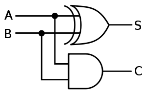
A logic circuit for the addition of two one-bit numbers is called a half adder. There must be two bits output: the sum of the addition (either a 1 or 0) and whether or not you carry a bit. The carry comes from the addition of 1 + 1, which equals 10 (binary 2). The addition process is reproduced in this truth table.
| A | B | Sum | Carry |
|---|---|---|---|
| 0 | 1 | 1 | 0 |
| 1 | 0 | 1 | 0 |
| 1 | 1 | 0 | 1 |
Multiplexers
BOOLEAN EXPRESSION:
D0 = X’Y’  ,  D1 = X’Y
D2 = XY’  ,  D3 = XY