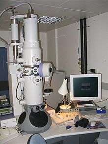
Electron microscope
An electron microscope is a microscope that uses a beam of accelerated electrons as a source of illumination. As the wavelength of an electron can be up to 100,000 times shorter than that of visible light photons, electron microscopes have a higher resolving power than light microscopes and can reveal the structure of smaller objects. A scanning transmission electron microscope has achieved better than 50 pm resolution in annular dark-field imaging mode[1] and magnifications of up to about 10,000,000× whereas most light microscopes are limited by diffraction to about 200 nm resolution and useful magnifications below 2000×.
Electron microscopes use shaped magnetic fields to form electron optical lens systems that are analogous to the glass lenses of an optical light microscope.
Electron microscopes are used to investigate the ultrastructure of a wide range of biological and inorganic specimens including microorganisms, cells, large molecules, biopsy samples, metals, and crystals. Industrially, electron microscopes are often used for quality control and failure analysis. Modern electron microscopes produce electron micrographs using specialized digital cameras and frame grabbers to capture the images.
History
In 1926 Hans Busch developed the electromagnetic lens.
According to Dennis Gabor, the physicist Leó Szilárd tried in 1928 to convince him to build an electron microscope, for which he had filed a patent.[2] The first prototype electron microscope, capable of four-hundred-power magnification, was developed in 1931 by the physicist Ernst Ruska and the electrical engineer Max Knoll.[3] The apparatus was the first practical demonstration of the principles of electron microscopy.[4] In May of the same year, Reinhold Rudenberg, the scientific director of Siemens-Schuckertwerke, obtained a patent for an electron microscope. In 1932, Ernst Lubcke of Siemens & Halske built and obtained images from a prototype electron microscope, applying the concepts described in Rudenberg's patent.[5]
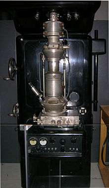
In the following year, 1933, Ruska built the first electron microscope that exceeded the resolution attainable with an optical (light) microscope.[4] Four years later, in 1937, Siemens financed the work of Ernst Ruska and Bodo von Borries, and employed Helmut Ruska, Ernst's brother, to develop applications for the microscope, especially with biological specimens.[4][6] Also in 1937, Manfred von Ardenne pioneered the scanning electron microscope.[7] Siemens produced the first commercial electron microscope in 1938.[8] The first North American electron microscope was constructed in 1938, at the University of Toronto, by Eli Franklin Burton and students Cecil Hall, James Hillier, and Albert Prebus. Siemens produced a transmission electron microscope (TEM) in 1939.[9] Although current transmission electron microscopes are capable of two million-power magnification, as scientific instruments, they remain based upon Ruska's prototype.
Types
Transmission electron microscope (TEM)
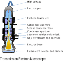
The original form of the electron microscope, the transmission electron microscope (TEM), uses a high voltage electron beam to illuminate the specimen and create an image. The electron beam is produced by an electron gun, commonly fitted with a tungsten filament cathode as the electron source. The electron beam is accelerated by an anode typically at +100 keV (40 to 400 keV) with respect to the cathode, focused by electrostatic and electromagnetic lenses, and transmitted through the specimen that is in part transparent to electrons and in part scatters them out of the beam. When it emerges from the specimen, the electron beam carries information about the structure of the specimen that is magnified by the objective lens system of the microscope. The spatial variation in this information (the "image") may be viewed by projecting the magnified electron image onto a fluorescent viewing screen coated with a phosphor or scintillator material such as zinc sulfide. Alternatively, the image can be photographically recorded by exposing a photographic film or plate directly to the electron beam, or a high-resolution phosphor may be coupled by means of a lens optical system or a fibre optic light-guide to the sensor of a digital camera. The image detected by the digital camera may be displayed on a monitor or computer.
The resolution of TEMs is limited primarily by spherical aberration, but a new generation of hardware correctors can reduce spherical aberration to increase the resolution in high-resolution transmission electron microscopy (HRTEM) to below 0.5 angstrom (50 picometres),[1] enabling magnifications above 50 million times.[10] The ability of HRTEM to determine the positions of atoms within materials is useful for nano-technologies research and development.[11]
Transmission electron microscopes are often used in electron diffraction mode. The advantages of electron diffraction over X-ray crystallography are that the specimen need not be a single crystal or even a polycrystalline powder, and also that the Fourier transform reconstruction of the object's magnified structure occurs physically and thus avoids the need for solving the phase problem faced by the X-ray crystallographers after obtaining their X-ray diffraction patterns.
One major disadvantage of the transmission electron microscope is the need for extremely thin sections of the specimens, typically about 100 nanometers. Creating these thin sections for biological and materials specimens is technically very challenging. Semiconductor thin sections can be made using a focused ion beam. Biological tissue specimens are chemically fixed, dehydrated and embedded in a polymer resin to stabilize them sufficiently to allow ultrathin sectioning. Sections of biological specimens, organic polymers, and similar materials may require staining with heavy atom labels in order to achieve the required image contrast.
Serial-section electron microscopy (ssEM)
One application of TEM is serial-section electron microscopy (ssEM), for example in analyzing the connectivity in volumetric samples of brain tissue by imaging many thin sections in sequence.[12]
Scanning electron microscope (SEM)

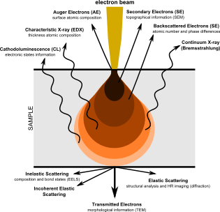
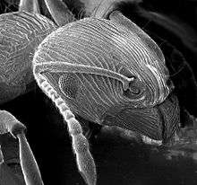
The SEM produces images by probing the specimen with a focused electron beam that is scanned across a rectangular area of the specimen (raster scanning). When the electron beam interacts with the specimen, it loses energy by a variety of mechanisms. The lost energy is converted into alternative forms such as heat, emission of low-energy secondary electrons and high-energy backscattered electrons, light emission (cathodoluminescence) or X-ray emission, all of which provide signals carrying information about the properties of the specimen surface, such as its topography and composition. The image displayed by an SEM maps the varying intensity of any of these signals into the image in a position corresponding to the position of the beam on the specimen when the signal was generated. In the SEM image of an ant shown below and to the right, the image was constructed from signals produced by a secondary electron detector, the normal or conventional imaging mode in most SEMs.
Generally, the image resolution of an SEM is lower than that of a TEM. However, because the SEM images the surface of a sample rather than its interior, the electrons do not have to travel through the sample. This reduces the need for extensive sample preparation to thin the specimen to electron transparency. The SEM is able to image bulk samples that can fit on its stage and still be maneuvered, including a height less than the working distance being used, often 4 millimeters for high-resolution images. The SEM also has a great depth of field, and so can produce images that are good representations of the three-dimensional surface shape of the sample. Another advantage of SEMs comes with environmental scanning electron microscopes (ESEM) that can produce images of good quality and resolution with hydrated samples or in low, rather than high, vacuum or under chamber gases. This facilitates imaging unfixed biological samples that are unstable in the high vacuum of conventional electron microscopes.
Reflection electron microscope (REM)
In the reflection electron microscope (REM) as in the TEM, an electron beam is incident on a surface but instead of using the transmission (TEM) or secondary electrons (SEM), the reflected beam of elastically scattered electrons is detected. This technique is typically coupled with reflection high energy electron diffraction (RHEED) and reflection high-energy loss spectroscopy (RHELS). Another variation is spin-polarized low-energy electron microscopy (SPLEEM), which is used for looking at the microstructure of magnetic domains.[13]
Scanning transmission electron microscope (STEM)
The STEM rasters a focused incident probe across a specimen that (as with the TEM) has been thinned to facilitate detection of electrons scattered through the specimen. The high resolution of the TEM is thus possible in STEM. The focusing action (and aberrations) occur before the electrons hit the specimen in the STEM, but afterward in the TEM. The STEMs use of SEM-like beam rastering simplifies annular dark-field imaging, and other analytical techniques, but also means that image data is acquired in serial rather than in parallel fashion. Often TEM can be equipped with the scanning option and then it can function both as TEM and STEM.
Scanning tunneling microscopy (STM)
In STM, a conductive tip held at a voltage is brought near a surface, and a profile can be obtained based on the tunneling probability of an electron from the tip to the sample since it is a function of distance.
Color
In their most common configurations, electron microscopes produce images with a single brightness value per pixel, with the results usually rendered in grayscale.[14] However, often these images are then colorized through the use of feature-detection software, or simply by hand-editing using a graphics editor. This may be done to clarify structure or for aesthetic effect and generally does not add new information about the specimen.[15]
In some configurations information about several specimen properties is gathered per pixel, usually by the use of multiple detectors.[16] In SEM, the attributes of topography and material contrast can be obtained by a pair of backscattered electron detectors and such attributes can be superimposed in a single color image by assigning a different primary color to each attribute.[17] Similarly, a combination of backscattered and secondary electron signals can be assigned to different colors and superimposed on a single color micrograph displaying simultaneously the properties of the specimen.[18]
Some types of detectors used in SEM have analytical capabilities, and can provide several items of data at each pixel. Examples are the Energy-dispersive X-ray spectroscopy (EDS) detectors used in elemental analysis and Cathodoluminescence microscope (CL) systems that analyse the intensity and spectrum of electron-induced luminescence in (for example) geological specimens. In SEM systems using these detectors, it is common to color code the signals and superimpose them in a single color image, so that differences in the distribution of the various components of the specimen can be seen clearly and compared. Optionally, the standard secondary electron image can be merged with the one or more compositional channels, so that the specimen's structure and composition can be compared. Such images can be made while maintaining the full integrity of the original signal, which is not modified in any way.
Sample preparation
Materials to be viewed under an electron microscope may require processing to produce a suitable sample. The technique required varies depending on the specimen and the analysis required:
- Chemical fixation – for biological specimens aims to stabilize the specimen's mobile macromolecular structure by chemical crosslinking of proteins with aldehydes such as formaldehyde and glutaraldehyde, and lipids with osmium tetroxide.
- Negative stain – suspensions containing nanoparticles or fine biological material (such as viruses and bacteria) are briefly mixed with a dilute solution of an electron-opaque solution such as ammonium molybdate, uranyl acetate (or formate), or phosphotungstic acid. This mixture is applied to a suitably coated EM grid, blotted, then allowed to dry. Viewing of this preparation in the TEM should be carried out without delay for best results. The method is important in microbiology for fast but crude morphological identification, but can also be used as the basis for high-resolution 3D reconstruction using EM tomography methodology when carbon films are used for support. Negative staining is also used for observation of nanoparticles.
- Cryofixation – freezing a specimen so rapidly, in liquid ethane that the water forms vitreous (non-crystalline) ice. This preserves the specimen in a snapshot of its solution state. An entire field called cryo-electron microscopy has branched from this technique. With the development of cryo-electron microscopy of vitreous sections (CEMOVIS), it is now possible to observe samples from virtually any biological specimen close to its native state.
- Dehydration – or replacement of water with organic solvents such as ethanol or acetone, followed by critical point drying or infiltration with embedding resins. Also freeze drying.
- Embedding, biological specimens – after dehydration, tissue for observation in the transmission electron microscope is embedded so it can be sectioned ready for viewing. To do this the tissue is passed through a 'transition solvent' such as propylene oxide (epoxypropane) or acetone and then infiltrated with an epoxy resin such as Araldite, Epon, or Durcupan;[19] tissues may also be embedded directly in water-miscible acrylic resin. After the resin has been polymerized (hardened) the sample is thin sectioned (ultrathin sections) and stained – it is then ready for viewing.
- Embedding, materials – after embedding in resin, the specimen is usually ground and polished to a mirror-like finish using ultra-fine abrasives. The polishing process must be performed carefully to minimize scratches and other polishing artifacts that reduce image quality.
- Metal shadowing – Metal (e.g. platinum) is evaporated from an overhead electrode and applied to the surface of a biological sample at an angle.[20] The surface topography results in variations in the thickness of the metal that are seen as variations in brightness and contrast in the electron microscope image.
- Replication – A surface shadowed with metal (e.g. platinum, or a mixture of carbon and platinum) at an angle is coated with pure carbon evaporated from carbon electrodes at right angles to the surface. This is followed by removal of the specimen material (e.g. in an acid bath, using enzymes or by mechanical separation[21]) to produce a surface replica that records the surface ultrastructure and can be examined using transmission electron microscopy.
- Sectioning – produces thin slices of the specimen, semitransparent to electrons. These can be cut on an ultramicrotome with a glass or diamond knife to produce ultra-thin sections about 60–90 nm thick. Disposable glass knives are also used because they can be made in the lab and are much cheaper.
- Staining – uses heavy metals such as lead, uranium or tungsten to scatter imaging electrons and thus give contrast between different structures, since many (especially biological) materials are nearly "transparent" to electrons (weak phase objects). In biology, specimens can be stained "en bloc" before embedding and also later after sectioning. Typically thin sections are stained for several minutes with an aqueous or alcoholic solution of uranyl acetate followed by aqueous lead citrate.[22]
- Freeze-fracture or freeze-etch – a preparation method[23][24] particularly useful for examining lipid membranes and their incorporated proteins in "face on" view.[25] The fresh tissue or cell suspension is frozen rapidly (cryofixation), then fractured by breaking[26] or by using a microtome while maintained at liquid nitrogen temperature. The cold fractured surface (sometimes "etched" by increasing the temperature to about −100 °C for several minutes to let some ice sublime) is then shadowed with evaporated platinum or gold at an average angle of 45° in a high vacuum evaporator. The second coat of carbon, evaporated perpendicular to the average surface plane is often performed to improve the stability of the replica coating. The specimen is returned to room temperature and pressure, then the extremely fragile "pre-shadowed" metal replica of the fracture surface is released from the underlying biological material by careful chemical digestion with acids, hypochlorite solution or SDS detergent. The still-floating replica is thoroughly washed free from residual chemicals, carefully fished up on fine grids, dried then viewed in the TEM.
- Freeze-fracture replica immunogold labeling (FRIL) – the freeze-fracture method has been modified to allow the identification of the components of the fracture face by immunogold labeling. Instead of removing all the underlying tissue of the thawed replica as the final step before viewing in the microscope the tissue thickness is minimized during or after the fracture process. The thin layer of tissue remains bound to the metal replica so it can be immunogold labeled with antibodies to the structures of choice. The thin layer of the original specimen on the replica with gold attached allows the identification of structures in the fracture plane.[27] There are also related methods which label the surface of etched cells[28] and other replica labeling variations.[29]
- Ion beam milling – thins samples until they are transparent to electrons by firing ions (typically argon) at the surface from an angle and sputtering material from the surface. A subclass of this is focused ion beam milling, where gallium ions are used to produce an electron transparent membrane in a specific region of the sample, for example through a device within a microprocessor. Ion beam milling may also be used for cross-section polishing prior to SEM analysis of materials that are difficult to prepare using mechanical polishing.
- Conductive coating – an ultrathin coating of electrically conducting material, deposited either by high vacuum evaporation or by low vacuum sputter coating of the sample. This is done to prevent the accumulation of static electric fields at the specimen due to the electron irradiation required during imaging. The coating materials include gold, gold/palladium, platinum, tungsten, graphite, etc.
- Earthing – to avoid electrical charge accumulation on a conductively coated sample, it is usually electrically connected to the metal sample holder. Often an electrically conductive adhesive is used for this purpose.
Disadvantages
Electron microscopes are expensive to build and maintain, but the capital and running costs of confocal light microscope systems now overlaps with those of basic electron microscopes. Microscopes designed to achieve high resolutions must be housed in stable buildings (sometimes underground) with special services such as magnetic field canceling systems.
The samples largely have to be viewed in vacuum, as the molecules that make up air would scatter the electrons. An exception is liquid-phase electron microscopy [30] using either a closed liquid cell or an environmental chamber, for example, in the environmental scanning electron microscope, which allows hydrated samples to be viewed in a low-pressure (up to 20 Torr or 2.7 kPa) wet environment. Various techniques for in situ electron microscopy of gaseous samples have been developed as well.[31]
Scanning electron microscopes operating in conventional high-vacuum mode usually image conductive specimens; therefore non-conductive materials require conductive coating (gold/palladium alloy, carbon, osmium, etc.). The low-voltage mode of modern microscopes makes possible the observation of non-conductive specimens without coating. Non-conductive materials can be imaged also by a variable pressure (or environmental) scanning electron microscope.
Small, stable specimens such as carbon nanotubes, diatom frustules and small mineral crystals (asbestos fibres, for example) require no special treatment before being examined in the electron microscope. Samples of hydrated materials, including almost all biological specimens have to be prepared in various ways to stabilize them, reduce their thickness (ultrathin sectioning) and increase their electron optical contrast (staining). These processes may result in artifacts, but these can usually be identified by comparing the results obtained by using radically different specimen preparation methods. Since the 1980s, analysis of cryofixed, vitrified specimens has also become increasingly used by scientists, further confirming the validity of this technique.[32][33][34]
Applications
Biology and life sciences
|
|
See also
- Acronyms in microscopy
- Electron diffraction
- Electron energy loss spectroscopy (EELS)
- Electron microscope images
- Energy filtered transmission electron microscopy (EFTEM)
- Environmental scanning electron microscope (ESEM)
- Field emission microscope
- HiRISE
- Immune electron microscopy
- In situ electron microscopy
- Microscope image processing
- Microscopy
- Nanoscience
- Nanotechnology
- Neutron microscope
- Quantum microscopy
- Scanning confocal electron microscopy
- Scanning electron microscope (SEM)
- Scanning tunneling microscope
- Surface science
- Transmission Electron Aberration-Corrected Microscope
- X-ray diffraction
- X-ray microscope
- Low-energy electron microscopy
- Hemispherical electron energy analyzer
References
- Erni, Rolf; Rossell, MD; Kisielowski, C; Dahmen, U (2009). "Atomic-Resolution Imaging with a Sub-50-pm Electron Probe". Physical Review Letters. 102 (9): 096101. Bibcode:2009PhRvL.102i6101E. doi:10.1103/PhysRevLett.102.096101. PMID 19392535.
- Dannen, Gene (1998) Leo Szilard the Inventor: A Slideshow (1998, Budapest, conference talk). dannen.com
- Mathys, Daniel, Zentrum für Mikroskopie, University of Basel: Die Entwicklung der Elektronenmikroskopie vom Bild über die Analyse zum Nanolabor, p. 8
- Ruska, Ernst (1986). "Ernst Ruska Autobiography". Nobel Foundation. Retrieved 2010-01-31.
- Rudenberg, H. Gunther; Rudenberg, Paul G. (2010). "Origin and Background of the Invention of the Electron Microscope". Advances in Imaging and Electron Physics. 160. pp. 207–286. doi:10.1016/S1076-5670(10)60006-7. ISBN 978-0-12-381017-5.
- Kruger, DH; Schneck, P; Gelderblom, HR (May 2000). "Helmut Ruska and the visualisation of viruses". The Lancet. 355 (9216): 1713–1717. doi:10.1016/S0140-6736(00)02250-9. PMID 10905259.
- Ardenne, M. Von; Beischer, D. (1940). "Untersuchung von Metalloxyd-Rauchen mit dem Universal-Elektronenmikroskop" [Investigation of metal oxide smoking with the universal electron microscope]. Zeitschrift für Elektrochemie und Angewandte Physikalische Chemie (in German). 46 (4): 270–277. doi:10.1002/bbpc.19400460406 (inactive 2020-03-09).
- History of electron microscopy, 1931–2000. Authors.library.caltech.edu (2002-12-10). Retrieved on 2017-04-29.
- "James Hillier". Inventor of the Week: Archive. 2003-05-01. Retrieved 2010-01-31.
- "The Scale of Things". Office of Basic Energy Sciences, U.S. Department of Energy. 2006-05-26. Archived from the original on 2010-02-01. Retrieved 2010-01-31.
- O'Keefe MA; Allard LF (2004-01-18). "Sub-Ångstrom Electron Microscopy for Sub-Ångstrom Nano-Metrology" (PDF). Information Bridge: DOE Scientific and Technical Information – Sponsored by OSTI. Cite journal requires
|journal=(help) - Yoo, Inwan, David GC Hildebrand, Willie F. Tobin, Wei-Chung Allen Lee, and Won-Ki Jeong. "ssEMnet: Serial-section Electron Microscopy Image Registration using a Spatial Transformer Network with Learned Features" In Deep Learning in Medical Image Analysis and Multimodal Learning for Clinical Decision Support, pp. 249-257. Springer, Cham, 2017.
- "SPLEEM". National Center for Electron Microscopy (NCEM). Archived from the original on 2010-05-29. Retrieved 2010-01-31.
- Burgess, Jeremy (1987). Under the Microscope: A Hidden World Revealed. CUP Archive. p. 11. ISBN 978-0-521-39940-1.
- "Introduction to Electron Microscopy" (PDF). FEI Company. p. 15. Retrieved 12 December 2012.
- Antonovsky, A. (1984). "The application of colour to sem imaging for increased definition". Micron and Microscopica Acta. 15 (2): 77–84. doi:10.1016/0739-6260(84)90005-4.
- Danilatos, G.D. (1986). "Colour micrographs for backscattered electron signals in the SEM". Scanning. 9 (3): 8–18. doi:10.1111/j.1365-2818.1986.tb04287.x.
- Danilatos, G.D. (1986). "Environmental scanning electron microscopy in colour". Journal of Microscopy. 142: 317–325. doi:10.1002/sca.4950080104.
- Luft, J.H. (1961). "Improvements in epoxy resin embedding methods". The Journal of Biophysical and Biochemical Cytology. 9 (2). p. 409. PMC 2224998. PMID 13764136.
- Williams, R. C.; Wyckoff, R. W. (1945-06-08). "Electron shadow micrography of the tobacco mosaic virus protein". Science. 101 (2632): 594–596. Bibcode:1945Sci...101..594W. doi:10.1126/science.101.2632.594. PMID 17739444.
- Juniper, B.E.; Bradley, D.E. (1958). "The carbon replica technique in the study of the ultrastructure of leaf surfaces". Journal of Ultrastructure Research. 2 (1): 16–27. doi:10.1016/s0022-5320(58)90045-5.
- Reynolds, E. S. (1963). "The use of lead citrate at high pH as an electron-opaque stain in electron microscopy". Journal of Cell Biology. 17: 208–212. doi:10.1083/jcb.17.1.208. PMC 2106263. PMID 13986422.
- Meryman H.T. and Kafig E. (1955). The study of frozen specimens, ice crystals and ices crystal growth by electron microscopy. Naval Med. Res. Ints. Rept NM 000 018.01.09 Vol. 13 pp 529–544
- Steere, Russell L. (1957-01-25). "Electron microscopy of structural detail in frozen biological specimens". The Journal of Biophysical and Biochemical Cytology. 3 (1): 45–60. doi:10.1083/jcb.3.1.45. PMC 2224015. PMID 13416310.
- Moor H, Mühlethaler K (1963). "Fine structure in frozen-etched yeast cells". The Journal of Cell Biology. 17 (3): 609–628. doi:10.1083/jcb.17.3.609. PMC 2106217. PMID 19866628.
- Bullivant, Stanley; Ames, Adelbert (1966-06-01). "A simple freeze-fracture replication method for electron microscopy". The Journal of Cell Biology. 29 (3): 435–447. doi:10.1083/jcb.29.3.435. PMC 2106967. PMID 5962938.
- Gruijters, W. T.; Kistler, J; Bullivant, S; Goodenough, D. A. (1987-03-01). "Immunolocalization of MP70 in lens fiber 16-17-nm intercellular junctions". The Journal of Cell Biology. 104 (3): 565–572. doi:10.1083/jcb.104.3.565. PMC 2114558. PMID 3818793.
- da Silva, Pedro Pinto; Branton, Daniel (1970-06-01). "Membrane splitting in freeze-etching". The Journal of Cell Biology. 45 (3): 598–605. doi:10.1083/jcb.45.3.598. PMC 2107921. PMID 4918216.
- Rash, J. E.; Johnson, T. J.; Hudson, C. S.; Giddings, F. D.; Graham, W. F.; Eldefrawi, M. E. (1982-11-01). "Labelled-replica techniques: post-shadow labelling of intramembrane particles in freeze-fracture replicas". Journal of Microscopy. 128 (Pt 2): 121–138. doi:10.1111/j.1365-2818.1982.tb00444.x. PMID 6184475.
- de Jonge, N.; Ross, F.M. (2011). "Electron microscopy of specimens in liquid". Nature Nanotechnology. 6 (8): 695–704. Bibcode:2003NatMa...2..532W. doi:10.1038/nmat944. PMID 12872162.
- Gai, P.L.; Boyes, E.D. (2009). "Advances in atomic resolution in situ environmental transmission electron microscopy and 1A aberration corrected in situ electron microscopy". Microsc Res Tech. 72 (3): 153–164. arXiv:1705.05754. doi:10.1002/jemt.20668. PMID 19140163.
- Adrian, Marc; Dubochet, Jacques; Lepault, Jean; McDowall, Alasdair W. (1984). "Cryo-electron microscopy of viruses". Nature (Submitted manuscript). 308 (5954): 32–36. Bibcode:1984Natur.308...32A. doi:10.1038/308032a0. PMID 6322001.
- Sabanay, I.; Arad, T.; Weiner, S.; Geiger, B. (1991). "Study of vitrified, unstained frozen tissue sections by cryoimmunoelectron microscopy". Journal of Cell Science. 100 (1): 227–236. PMID 1795028.
- Kasas, S.; Dumas, G.; Dietler, G.; Catsicas, S.; Adrian, M. (2003). "Vitrification of cryoelectron microscopy specimens revealed by high-speed photographic imaging". Journal of Microscopy. 211 (1): 48–53. doi:10.1046/j.1365-2818.2003.01193.x. PMID 12839550.
- Boehme, L.; Bresin, M.; Botman, A.; Ranney, J.; Hastings, J.T. (2015). "Focused electron beam induced etching of copper in sulfuric acid solutions". Nanotechnology. 26 (49): 495301. Bibcode:2015Nanot..26W5301B. doi:10.1088/0957-4484/26/49/495301. PMID 26567988.
- Kacher, J.; Cui, B.; Robertson, I.M. (2015). "In situ and tomographic characterization of damage and dislocation processes in irradiated metallic alloys by transmission electron microscopy". Journal of Materials Research. 30 (9): 1202–1213. Bibcode:2015JMatR..30.1202K. doi:10.1557/jmr.2015.14.
- Rai, R.S.; Subramanian, S. (2009). "Role of transmission electron microscopy in the semiconductor industry for process development and failure analysis". Progress in Crystal Growth and Characterization of Materials. 55 (3–4): 63–97. doi:10.1016/j.pcrysgrow.2009.09.002.
- Morris, G.J.; Goodrich, M.; Acton, E.; Fonseca, F. (2006). "The high viscosity encountered during freezing in glycerol solutions: Effects on cryopreservation". Cryobiology. 52 (3): 323–334. doi:10.1016/j.cryobiol.2006.01.003. PMID 16499898.
- von Appen, Alexander; Beck, Martin (May 2016). "Structure Determination of the Nuclear Pore Complex with Three-Dimensional Cryo electron Microscopy". Journal of Molecular Biology. 428 (10): 2001–10. doi:10.1016/j.jmb.2016.01.004. PMC 4898182. PMID 26791760.
- Florian, P.E.; Rouillé, Y.; Ruta, S.; Nichita, N.; Roseanu, A. (2016). "Recent advances in human viruses imaging studies". Journal of Basic Microbiology. 56 (6): 591–607. doi:10.1002/jobm.201500575. PMID 27059598.
- Cushnie, T.P.; O’Driscoll, N.H.; Lamb, A.J. (2016). "Morphological and ultrastructural changes in bacterial cells as an indicator of antibacterial mechanism of action". Cellular and Molecular Life Sciences. 73 (23): 4471–4492. doi:10.1007/s00018-016-2302-2. hdl:10059/2129. PMID 27392605.
- Li, M.-H.; Yang, Y.-Q.; Huang, B.; Luo, X.; Zhang, W.; Han, M.; Ru, J.-G. (2014). "Development of advanced electron tomography in materials science based on TEM and STEM". Transactions of Nonferrous Metals Society of China. 24 (10): 3031–3050. doi:10.1016/S1003-6326(14)63441-5.
- Li, W.J.; Shao, L.Y.; Zhang, D.Z.; Ro, C.U.; Hu, M.; Bi, X.H.; Geng, H.; Matsuki, A.; Niu, H.Y.; Chen, J.M. (2016). "A review of single aerosol particle studies in the atmosphere of East Asia: morphology, mixing state, source, and heterogeneous reactions". Journal of Cleaner Production. 112 (2): 1330–1349. doi:10.1016/j.jclepro.2015.04.050.
- Sousa, R.G.; Esteves, T.; Rocha, S.; Figueiredo, F.; Quelhas, P.; Silva, L.M. (2015). Automatic detection of immunogold particles from electron microscopy images. Image Analysis and Recognition. Lecture Notes in Computer Science. 9164. pp. 377–384. doi:10.1007/978-3-319-20801-5_41. ISBN 978-3-319-20800-8.
- Perkins, G.A. (2014). "The Use of miniSOG in the Localization of Mitochondrial Proteins". Mitochondrial Function. Methods in Enzymology. 547. pp. 165–179. doi:10.1016/B978-0-12-801415-8.00010-2. ISBN 9780128014158. PMID 25416358.
- Chen, X.D.; Ren, L.Q.; Zheng, B.; Liu, H. (2013). "Physics and engineering aspects of cell and tissue imaging systems: microscopic devices and computer assisted diagnosis". Biophotonics in Pathology: Pathology at the Crossroads. 185 (Biophotonics in Pathology): 1–22. doi:10.3233/978-1-61499-234-9-1. PMID 23542929.
- Fagerland, J.A.; Wall, H.G.; Pandher, K.; LeRoy, B.E.; Gagne, G.D. (2012). "Ultrastructural analysis in preclinical safety evaluation". Toxicologic Pathology. 40 (2): 391–402. doi:10.1177/0192623311430239. PMID 22215513.
- Heider, S.; Metzner, C. (2014). "Quantitative real-time single particle analysis of virions". Virology. 462–463: 199–206. doi:10.1016/j.virol.2014.06.005. PMC 4139191. PMID 24999044.
- Tsekouras, G.; Mozer, A.J.; Wallace, G.G. (2008). "Enhanced performance of dye sensitized solar cells utilizing platinum electrodeposit counter electrodes". Journal of the Electrochemical Society. 155 (7): K124–K128. doi:10.1149/1.2919107.
- Besenius, P.; Portale, G.; Bomans, P.H.H.; Janssen, H.M.; Palmans, A.R.A.; Meijer, E.W. (2010). "Controlling the growth and shape of chiral supramolecular polymers in water". Proceedings of the National Academy of Sciences of the United States of America. 107 (42): 17888–17893. Bibcode:2010PNAS..10717888B. doi:10.1073/pnas.1009592107. PMC 2964246. PMID 20921365.
- Furuya, K. (2008). "Nanofabrication by advanced electron microscopy using intense and focused beam". Science and Technology of Advanced Materials. 9 (1): Article 014110. Bibcode:2008STAdM...9a4110F. doi:10.1088/1468-6996/9/1/014110. PMC 5099805. PMID 27877936.
- Kosasih, Felix Utama; Ducati, Caterina (May 2018). "Characterising degradation of perovskite solar cells through in-situ and operando electron microscopy". Nano Energy. 47: 243–256. doi:10.1016/j.nanoen.2018.02.055.
- Maloy, Stuart A.; Sommer, Walter F.; James, Michael R.; Romero, Tobias J.; Lopez, Manuel R.; Zimmermann, Eugene; Ledbetter, James M. (13 May 2017). "The Accelerator Production of Tritium Materials Test Program". Nuclear Technology. 132 (1): 103–114. doi:10.13182/nt00-a3132.
- Ukraintsev, Vladimir (27 February 2012). "Review of reference metrology for nanotechnology: significance, challenges, and solutions". Journal of Micro/Nanolithography, MEMS, and MOEMS. 11 (1): 011010. doi:10.1117/1.JMM.11.1.011010.
- Wilhelmi, O.; Roussel, L.; Faber, P.; Reyntjens, S.; Daniel, G. (June 2010). "Focussed ion beam fabrication of large and complex nanopatterns". Journal of Experimental Nanoscience. 5 (3): 244–250. Bibcode:2010JENan...5..244W. doi:10.1080/17458080903487448.
- Vogt, E.T.C.; Whiting, G.T.; Chowdhury, A.D.; Weckhuysen, B.M. (2015). Zeolites and zeotypes for oil and gas conversion. Advances in Catalysis. 58. pp. 143–314. doi:10.1016/bs.acat.2015.10.001. ISBN 9780128021262.
- Lai, Shih-En; Hong, Ying-Jhan; Chen, Yu-Ting; Kang, Yu-Ting; Chang, Pin; Yew, Tri-Rung (18 September 2015). "Direct-Writing of Cu Nano-Patterns with an Electron Beam". Microscopy and Microanalysis. 21 (6): 1639–43. Bibcode:2015MiMic..21.1639L. doi:10.1017/S1431927615015111. PMID 26381450.
- Sicignano, Angelo; Di Monaco, Rossella; Masi, Paolo; Cavella, Silvana (October 2015). "From raw material to dish: pasta quality step by step". Journal of the Science of Food and Agriculture. 95 (13): 2579–87. doi:10.1002/jsfa.7176. PMID 25783568.
- Brożek-Mucha, Zuzanna (2014). "Scanning Electron Microscopy and X-Ray Microanalysis for Chemical and Morphological Characterisation of the Inorganic Component of Gunshot Residue: Selected Problems". BioMed Research International. 2014: 428038. doi:10.1155/2014/428038. PMC 4082842. PMID 25025050.
- Carbonell-Verdu, A.; Garcia-Sanoguera, D.; Jorda-Vilaplana, A.; Sanchez-Nacher, L.; Balart, R. (2016). "A new biobased plasticizer for poly(vinyl chloride) based on epoxidized cottonseed oil". Journal of Applied Polymer Science. 33 (27): 43642. doi:10.1002/app.43642. hdl:10251/82834.
- Ding, Jie; Zhang, Zhiming (1 May 2015). "Micro-characterization of dissimilar metal weld joint for connecting pipe-nozzle to safe-end in generation III nuclear power plant". Acta Metall Sin. 51 (4): 425–39. doi:10.11900/0412.1961.2014.00299 (inactive 2020-03-09).
- Tsikouras, Basilios; Pe-Piper, Georgia; Piper, David J.W.; Schaffer, Michael (June 2011). "Varietal heavy mineral analysis of sediment provenance, Lower Cretaceous Scotian Basin, eastern Canada". Sedimentary Geology. 237 (3–4): 150–165. Bibcode:2011SedG..237..150T. doi:10.1016/j.sedgeo.2011.02.011.
- Li, Xiang; Jiang, Chuan; Pan, Lili; Zhang, Haoyang; Hu, Lang; Li, Tianxue; Yang, Xinghao (15 July 2014). "Effects of preparing techniques and aging on dissolution behavior of the solid dispersions of NF/Soluplus/Kollidon SR: identification and classification by a combined analysis by FT-IR spectroscopy and computational approaches". Drug Development and Industrial Pharmacy. 41 (1): 2–14. doi:10.3109/03639045.2014.938080. PMID 25026247.
External links
| Library resources about Electron microscopy |
| Wikimedia Commons has media related to Electron microscopes. |
- An Introduction to Electron Microscopy: resources for teachers and students
- Cell Centered Database – Electron microscopy data
- Science Aid: Electron Microscopy: high school (GCSE, A Level) resource
General
- Animations and explanations of various types of microscopy including electron microscopy (Université Paris Sud)
- Environmental Scanning Electron Microscopy (ESEM)
- ETH Zurich website: graphics and images illustrating various procedures
- Eva Nogales's Seminar: "Introduction to Electron Microscopy"
- FEI Image Contest: FEI has had a microscopy image contest every year since 2008
- Introduction to electron microscopy by David Szondy
- Nanohedron.com image gallery: images generated by electron microscopy
- X-ray element analysis in electron microscopy: information portal with X-ray microanalysis and EDX contents
History
- John H.L. Watson's recollections at the University of Toronto when he worked with Hillier and Prebus
- Rubin Borasky Electron Microscopy Collection, 1930–1988 (Archives Center, National Museum of American History, Smithsonian Institution)