Self-assembled monolayer
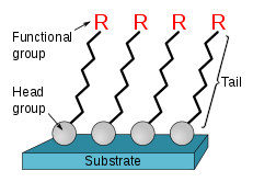
Self-assembled monolayers (SAM) of organic molecules are molecular assemblies formed spontaneously on surfaces by adsorption and are organized into more or less large ordered domains.[1][2] In some cases molecules that form the monolayer do not interact strongly with the substrate. This is the case for instance of the two-dimensional supramolecular networks[3] of e.g. perylenetetracarboxylic dianhydride (PTCDA) on gold[4] or of e.g. porphyrins on highly oriented pyrolitic graphite (HOPG).[5] In other cases the molecules possess a head group that has a strong affinity to the substrate and anchors the molecule to it.[1] Such a SAM consisting of a head group, tail and functional end group is depicted in Figure 1. Common head groups include thiols, silanes, phosphonates, etc.
| Part of a series of articles on |
| Molecular self-assembly |
|---|
 |
|
SAMs are created by the chemisorption of "head groups" onto a substrate from either the vapor or liquid phase[6][7] followed by a slow organization of "tail groups".[8] Initially, at small molecular density on the surface, adsorbate molecules form either a disordered mass of molecules or form an ordered two-dimensional "lying down phase",[6] and at higher molecular coverage, over a period of minutes to hours, begin to form three-dimensional crystalline or semicrystalline structures on the substrate surface.[9] The "head groups" assemble together on the substrate, while the tail groups assemble far from the substrate. Areas of close-packed molecules nucleate and grow until the surface of the substrate is covered in a single monolayer.
Adsorbate molecules adsorb readily because they lower the surface free-energy of the substrate[1] and are stable due to the strong chemisorption of the "head groups." These bonds create monolayers that are more stable than the physisorbed bonds of Langmuir–Blodgett films.[10][11] A Trichlorosilane based "head group", for example in a FDTS molecule, reacts with a hydroxyl group on a substrate, and forms very stable, covalent bond [R-Si-O-substrate] with an energy of 452 kJ/mol. Thiol-metal bonds are on the order of 100 kJ/mol, making them fairly stable in a variety of temperatures, solvents, and potentials.[9] The monolayer packs tightly due to van der Waals interactions,[1][11] thereby reducing its own free energy.[1] The adsorption can be described by the Langmuir adsorption isotherm if lateral interactions are neglected. If they cannot be neglected, the adsorption is better described by the Frumkin isotherm.[9]
Types
Selecting the type of head group depends on the application of the SAM.[1] Typically, head groups are connected to a molecular chain in which the terminal end can be functionalized (i.e. adding –OH, –NH2, –COOH, or –SH groups) to vary the wetting and interfacial properties.[10][12] An appropriate substrate is chosen to react with the head group. Substrates can be planar surfaces, such as silicon and metals, or curved surfaces, such as nanoparticles. Alkanethiols are the most commonly used molecules for SAMs. Alkanethiols are molecules with an alkyl chain, (C-C)ⁿ chain, as the back bone, a tail group, and a S-H head group. Other types of interesting molecules include aromatic thiols, of interest in molecular electronics, in which the alkane chain is (partly) replaced by aromatic rings. An example is the dithiol 1,4-Benzenedimethanethiol (SHCH2C6H4CH2SH)). Interest in such dithiols stems from the possibility of linking the two sulfur ends to metallic contacts, which was first used in molecular conduction measurements.[13] Thiols are frequently used on noble metal substrates because of the strong affinity of sulfur for these metals. The sulfur gold interaction is semi-covalent and has a strength of approximately 45kcal/mol. In addition, gold is an inert and biocompatible material that is easy to acquire. It is also easy to pattern via lithography, a useful feature for applications in nanoelectromechanical systems (NEMS).[1] Additionally, it can withstand harsh chemical cleaning treatments.[9] Recently other chalcogenide SAMs: selenides and tellurides have attracted attention[14][15] in a search for different bonding characteristics to substrates affecting the SAM characteristics and which could be of interest in some applications such as molecular electronics. Silanes are generally used on nonmetallic oxide surfaces;[1] however monolayers formed from covalent bonds between silicon and carbon or oxygen cannot be considered self assembled because they do not form reversibly. Self-assembled monolayers of thiolates on noble metals are a special case because the metal-metal bonds become reversible after the formation of the thiolate-metal complex.[16] This reversibility is what gives rise to vacancy islands and it is why SAMs of alkanethiolates can be thermally desorbed and undergo exchange with free thiols.[17]
Preparation
Metal substrates for use in SAMs can be produced through physical vapor deposition techniques, electrodeposition or electroless deposition.[1] Thiol or selenium SAMs produced by adsorption from solution are typically made by immersing a substrate into a dilute solution of alkane thiol in ethanol, though many different solvents can be used[1] besides use of pure liquids.[15] While SAMs are often allowed to form over 12 to 72 hours at room temperature,[9][18] SAMs of alkanethiolates form within minutes.[19][20] Special attention is essential in some cases, such as that of dithiol SAMs to avoid problems due to oxidation or photoinduced processes, which can affect terminal groups and lead to disorder and multilayer formation.[21][22] In this case appropriate choice of solvents, their degassing by inert gasses and preparation in the absence of light is crucial[21][22] and allows formation of "standing up" SAMs with free –SH groups. Self-assembled monolayers can also be adsorbed from the vapor phase.[7][23] In some cases when obtaining an ordered assembly is difficult or when different density phases need to be obtained substitutional self-assembly is used. Here one first forms the SAM of a given type of molecules, which give rise to ordered assembly and then a second assembly phase is performed (e.g. by immersion into a different solution). This method has also been used to give information on relative binding strengths of SAMs with different head groups and more generally on self-assembly characteristics.[17][24]
Characterization
The thicknesses of SAMs can be measured using ellipsometry and X-ray photoelectron spectroscopy (XPS), which also give information on interfacial properties.[21][25] The order in the SAM and orientation of molecules can be probed by Near Edge Xray Absorption Fine Structure (NEXAFS) and Fourier Transform Infrared Spectroscopy in Reflection Absorption Infrared Spectroscopy (RAIRS)[19][22] studies. Numerous other spectroscopic techniques are used[7] such as Second-harmonic generation (SHG), Sum-frequency generation (SFG), Surface-enhanced Raman scattering (SERS), as well as[26] High-resolution electron energy loss spectroscopy (HREELS). The structures of SAMs are commonly determined using scanning probe microscopy techniques such as atomic force microscopy (AFM) and scanning tunneling microscopy (STM). STM has been able to help understand the mechanisms of SAM formation as well as determine the important structural features that lend SAMs their integrity as surface-stable entities. In particular STM can image the shape, spatial distribution, terminal groups and their packing structure. AFM offers an equally powerful tool without the requirement of the SAM being conducting or semi-conducting. AFM has been used to determine chemical functionality, conductance, magnetic properties, surface charge, and frictional forces of SAMs.[27] The scanning vibrating electrode technique (SVET) is a further scanning probe microscopy which has been used to characterize SAMs, with defect free SAMs showing homogeneous activity in SVET.[28] More recently, however, diffractive methods have also been used.[1] The structure can be used to characterize the kinetics and defects found on the monolayer surface. These techniques have also shown physical differences between SAMs with planar substrates and nanoparticle substrates. An alternative characterisation instrument for measuring the self-assembly in real time is dual polarisation interferometry where the refractive index, thickness, mass and birefringence of the self assembled layer are quantified at high resolution. Contact angle measurements can be used to determine the surface free-energy which reflects the average composition of the surface of the SAM and can be used to probe the kinetics and thermodynamics of the formation of SAMs.[19][20] The kinetics of adsorption and temperature induced desorption as well as information on structure can also be obtained in real time by ion scattering techniques such as low energy ion scattering (LEIS) and time of flight direct recoil spectroscopy (TOFDRS).[23]
Defects
Defects due to both external and intrinsic factors may appear. External factors include the cleanliness of the substrate, method of preparation, and purity of the adsorbates.[1][9] SAMs intrinsically form defects due to the thermodynamics of formation, e.g. thiol SAMs on gold typically exhibit etch pits (monatomic vacancy islands) likely due to extraction of adatoms from the substrate and formation of adatom-adsorbate moieties. Recently, a new type of fluorosurfactants have found that can form nearly perfect monolayer on gold substrate due to the increase of mobility of gold surface atoms.[29][30][31]
Nanoparticle properties
The structure of SAMs is also dependent on the curvature of the substrate. SAMs on nanoparticles, including colloids and nanocrystals, "stabilize the reactive surface of the particle and present organic functional groups at the particle-solvent interface".[1] These organic functional groups are useful for applications, such as immunoassays or sensors, that are dependent on chemical composition of the surface.[1]
Kinetics
There is evidence that SAM formation occurs in two steps: an initial fast step of adsorption and a second slower step of monolayer organization. Adsorption occurs at the liquid–liquid, liquid–vapor, and liquid-solid interfaces. The transport of molecules to the surface occurs due to a combination of diffusion and convective transport. According to the Langmuir or Avrami kinetic model the rate of deposition onto the surface is proportional to the free space of the surface.[6]

Where θ is the proportional amount of area deposited and k is the rate constant. Although this model is robust it is only used for approximations because it fails to take into account intermediate processes.[6] Dual polarisation interferometry being a real time technique with ~10 Hz resolution can measure the kinetics of monolayer self-assembly directly.
Once the molecules are at the surface the self-organization occurs in three phases:[6]
- 1. A low-density phase with random dispersion of molecules on the surface.
- 2. An intermediate-density phase with conformational disordered molecules or molecules lying flat on the surface.
- 3. A high-density phase with close-packed order and molecules standing normal to the substrate's surface.
The phase transitions in which a SAM forms depends on the temperature of the environment relative to the triple point temperature, the temperature in which the tip of the low-density phase intersects with the intermediate-phase region. At temperatures below the triple point the growth goes from phase 1 to phase 2 where many islands form with the final SAM structure, but are surrounded by random molecules. Similar to nucleation in metals, as these islands grow larger they intersect forming boundaries until they end up in phase 3, as seen below.[6]
At temperatures above the triple point the growth is more complex and can take two paths. In the first path the heads of the SAM organize to their near final locations with the tail groups loosely formed on top. Then as they transit to phase 3, the tail groups become ordered and straighten out. In the second path the molecules start in a lying down position along the surface. These then form into islands of ordered SAMs, where they grow into phase 3, as seen below.[6]
The nature in which the tail groups organize themselves into a straight ordered monolayer is dependent on the inter-molecular attraction, or van der Waals forces, between the tail groups. To minimize the free energy of the organic layer the molecules adopt conformations that allow high degree of Van der Waals forces with some hydrogen bonding. The small size of the SAM molecules are important here because Van der Waals forces arise from the dipoles of molecules and are thus much weaker than the surrounding surface forces at larger scales. The assembly process begins with a small group of molecules, usually two, getting close enough that the Van der Waals forces overcome the surrounding force. The forces between the molecules orient them so they are in their straight, optimal, configuration. Then as other molecules come close by they interact with these already organized molecules in the same fashion and become a part of the conformed group. When this occurs across a large area the molecules support each other into forming their SAM shape seen in Figure 1. The orientation of the molecules can be described with two parameters: α and β. α is the angle of tilt of the backbone from the surface normal. In typical applications α varies from 0 to 60 degrees depending on the substrate and type of SAM molecule. β is the angle of rotation along the long axis of tee molecule. β is usually between 30 and 40 degrees.[1] In some cases existence of kinetic traps hindering the final ordered orientation has been pointed out.[7] Thus in case of dithiols formation of a "lying down" phase[7] was considered an impediment to formation of "standing up" phase, however various recent studies indicate this is not the case.[21][22]
Many of the SAM properties, such as thickness, are determined in the first few minutes. However, it may take hours for defects to be eliminated via annealing and for final SAM properties to be determined.[6][9] The exact kinetics of SAM formation depends on the adsorbate, solvent and substrate properties. In general, however, the kinetics are dependent on both preparations conditions and material properties of the solvent, adsorbate and substrate.[6] Specifically, kinetics for adsorption from a liquid solution are dependent on:[1]
- Temperature – room-temperature preparation improves kinetics and reduces defects.
- Concentration of adsorbate in the solution – low concentrations require longer immersion times[1][9] and often create highly crystalline domains.[9]
- Purity of the adsorbate – impurities can affect the final physical properties of the SAM
- Dirt or contamination on the substrate – imperfections can cause defects in the SAM
The final structure of the SAM is also dependent on the chain length and the structure of both the adsorbate and the substrate. Steric hindrance and metal substrate properties, for example, can affect the packing density of the film,[1][9] while chain length affects SAM thickness.[11] Longer chain length also increases the thermodynamic stability.[1]
Patterning
1. Locally attract
This first strategy involves locally depositing self-assembled monolayers on the surface only where the nanostructure will later be located. This strategy is advantageous because it involves high throughput methods that generally involve fewer steps than the other two strategies. The major techniques that use this strategy are:[32]
- Micro-contact printing or soft lithography is analogous to printing ink with a rubber stamp. The SAM molecules are inked onto a pre-shaped elastomeric stamp with a solvent and transferred to the substrate surface by stamping. The SAM solution is applied to the entire stamp but only areas that make contact with the surface allow transfer of the SAMs. The transfer of the SAMs is a complex diffusion process that depends on the type of molecule, concentration, duration of contact, and pressure applied. Typical stamps use PDMS because its elastomeric properties, E = 1.8 MPa, allow it to fit the countour of micro surfaces and its low surface energy, γ = 21.6 dyn/cm². This is a parallel process and can thus place nanoscale objects over a large area in a short time.[1]
- Dip-pen nanolithography is a process that uses an atomic force microscope to transfer molecules on the tip to a substrate. Initially the tip is dipped into a reservoir with an ink. The ink on the tip evaporates and leaves the desired molecules attached to the tip. When the tip is brought into contact with the surface a water meniscus forms between the tip and the surface resulting in the diffusion of molecules from the tip to the surface. These tips can have radii in the tens of nanometers, and thus SAM molecules can be very precisely deposited onto a specific location of the surface. This process was discovered by Chad Mirkin and co-workers at Northwestern University.[33]
2. Locally remove
The locally remove strategy begins with covering the entire surface with a SAM. Then individual SAM molecules are removed from locations where the deposition of nanostructures is not desired. The end result is the same as in the locally attract strategy, the difference being in the way this is achieved. The major techniques that use this strategy are:[32]
- The scanning tunneling microscope can remove SAM molecules in many different ways. The first is to remove them mechanically by dragging the tip across the substrate surface. This is not the most desired technique as these tips are expensive and dragging them causes a lot of wear and reduction of the tip quality. The second way is to degrade or desorb the SAM molecules by shooting them with an electron beam. The scanning tunneling microscope can also remove SAMs by field desorption and field enhanced surface diffusion.[32]
- Atomic force microscope
- The most common use of this technique is to remove the SAM molecules in a process called shaving, where the atomic force microscope tip is dragged along the surface mechanically removing the molecules. An atomic force microscope can also remove SAM molecules by local oxidation nanolithography.[32]
- Ultraviolet irradiation
- In this process, UV light is projected onto the surface with a SAM through a pattern of apperatures in a chromium film. This leads to photo oxidation of the SAM molecules. These can then be washed away in a polar solvent. This process has 100 nm resolutions and requires exposure time of 15–20 minutes.[1]
3. Modify tail groups
The final strategy focuses not on the deposition or removal of SAMS, but the modification of terminal groups. In the first case the terminal group can be modified to remove functionality so that SAM molecule will be inert. In the same regards the terminal group can be modified to add functionality[34] so it can accept different materials or have different properties than the original SAM terminal group. The major techniques that use this strategy are:[32]
- Focused electron beam and ultraviolet irradiation
- Exposure to electron beams and UV light changes the terminal group chemistry. Some of the changes that can occur include the cleavage of bonds, the forming of double carbon bonds, cross-linking of adjacent molecules, fragmentation of molecules, and confromational disorder.[1]
- Atomic force microscope
- A conductive AFM tip can create an electrochemical reaction that can change the terminal group.[32]
Applications
Thin-film SAMs
SAMs are an inexpensive and versatile surface coating for applications including control of wetting and adhesion,[35] chemical resistance, bio compatibility, sensitization, and molecular recognition for sensors[36] and nano fabrication.[6] Areas of application for SAMs include biology, electrochemistry and electronics, nanoelectromechanical systems (NEMS) and microelectromechanical systems (MEMS), and everyday household goods. SAMs can serve as models for studying membrane properties of cells and organelles and cell attachment on surfaces.[1] SAMs can also be used to modify the surface properties of electrodes for electrochemistry, general electronics, and various NEMS and MEMS.[1] For example, the properties of SAMs can be used to control electron transfer in electrochemistry.[37] They can serve to protect metals from harsh chemicals and etchants. SAMs can also reduce sticking of NEMS and MEMS components in humid environments. In the same way, SAMs can alter the properties of glass. A common household product, Rain-X, utilizes SAMs to create a hydrophobic monolayer on car windshields to keep them clear of rain. Another application is an anti-adhesion coating on nanoimprint lithography (NIL) tools and stamps. One can also coat injection molding tools for polymer replication with a Perfluordecyltrichlorosilane SAM.[38]
Thin film SAMs can also be placed on nanostructures. In this way they functionalize the nanostructure. This is advantageous because the nanostructure can now selectively attach itself to other molecules or SAMs. This technique is useful in biosensors or other MEMS devices that need to separate one type of molecule from its environment. One example is the use of magnetic nanoparticles to remove a fungus from a blood stream. The nanoparticle is coated with a SAM that binds to the fungus. As the contaminated blood is filtered through a MEMS device the magnetic nanoparticles are inserted into the blood where they bind to the fungus and are then magnetically driven out of the blood stream into a nearby laminar waste stream.[39]
Patterned SAMs
SAMs are also useful in depositing nanostructures, because each adsorbate molecule can be tailored to attract two different materials. Current techniques utilize the head to attract to a surface, like a plate of gold. The terminal group is then modified to attract a specific material like a particular nanoparticle, wire, ribbon, or other nanostructure. In this way, wherever the a SAM is patterned to a surface there will be nanostructures attached to the tail groups. One example is the use of two types of SAMs to align single wall carbon nanotubes, SWNTs. Dip pen nanolithography was used to pattern a 16-mercaptohexadecanoic acid (MHA)SAM and the rest of the surface was passivated with 1-octadecanethiol (ODT) SAM. The polar solvent that is carrying the SWNTs is attracted to the hydrophilic MHA; as the solvent evaporates, the SWNTs are close enough to the MHA SAM to attach to it due to Van der Waals forces. The nanotubes thus line up with the MHA-ODT boundary. Using this technique Chad Mirkin, Schatz and their co-workers were able to make complex two-dimensional shapes, a representation of a shape created is shown to the right.[32][40] Another application of patterned SAMs is the functionalization of biosensors. The tail groups can be modified so they have an affinity for cells, proteins, or molecules. The SAM can then be placed onto a biosensor so that binding of these molecules can be detected. The ability to pattern these SAMs allows them to be placed in configurations that increase sensitivity and do not damage or interfere with other components of the biosensor.[27]
References
- Love; et al. (2005). "Self-Assembled Monolayers of Thiolates on Metals as a Form of Nanotechnology". Chem. Rev. 105 (4): 1103–1170. doi:10.1021/cr0300789. PMID 15826011.
- Barlow, S.M.; Raval R.. (2003). "Complex organic molecules at metal surfaces: bonding, organisation and chirality". Surface Science Reports. 50 (6–8): 201–341. Bibcode:2003SurSR..50..201B. doi:10.1016/S0167-5729(03)00015-3.
- Elemans, J.A.A.W.; Lei S., De Feyter S. (2009). "Molecular and Supramolecular Networks on Surfaces: From Two-Dimensional Crystal Engineering to Reactivity". Angew. Chem. Int. Ed. 48 (40): 7298–7332. doi:10.1002/anie.200806339. PMID 19746490.
- Witte, G.; Wöll Ch. (2004). "Growth of aromatic molecules on solid substrates for applications in organic electronics". Journal of Materials Research. 19 (7): 1889–1916. Bibcode:2004JMatR..19.1889W. doi:10.1557/JMR.2004.0251.
- De Feyter, S.; De Schreyer F.C. (2003). "Two-dimensional supramolecular self-assembly probed by scanning tunneling microscopy". Chemical Society Reviews. 32 (3): 139–150. CiteSeerX 10.1.1.467.5727. doi:10.1039/b206566p. PMID 12792937.
- Schwartz, D.K., Mechanisms and Kinetics of Self-Assembled Monolayer Formation (2001). "Mechanisms and kinetics of self-assembled monolayer formation". Annu. Rev. Phys. Chem. 52: 107–37. Bibcode:2001ARPC...52..107S. doi:10.1146/annurev.physchem.52.1.107. PMID 11326061.CS1 maint: multiple names: authors list (link)
- Schreiber, F (30 November 2000). "Structure and growth of self-assembling monolayers". Progress in Surface Science. 65 (5–8): 151–257. Bibcode:2000PrSS...65..151S. doi:10.1016/S0079-6816(00)00024-1.
- Wnek, Gary, Gary L. Bowlin (2004). Encyclopedia of Biomaterials and Biomedical Engineering. Informa Healthcare. pp. 1331–1333.CS1 maint: multiple names: authors list (link)
- Vos, Johannes G., Robert J. Forster, Tia E. Keyes (2003). Interfacial Supramolecular Assemblies. Wiley. pp. 88–94.CS1 maint: multiple names: authors list (link)
- Madou, Marc (2002). Fundamentals of Microfabrication: The Science of Miniaturization. CRC. pp. 62–63.
- Kaifer, Angel (2001). Supramolecular Electrochemistry. Coral Gables. Wiley VCH. pp. 191–193.
- Saliterman, Steven (2006). Self-assembled monolayers (SAMs). Fundamentals of BioMEMS and Medical Microdevices. SPIE Press. pp. 94–96.
- Andres, R.P.; Bein T.; Dorogi M.; Feng S.; Henderson J.I.; Kubiak C.P.; Mahoney W.; Osifchin R.G.; Reifenberger R. (1996). "Coulomb Staircase at Room Temperature in a Self-Assembled Molecular Nanostructure". Science. 272 (5266): 1323–1325. Bibcode:1996Sci...272.1323A. doi:10.1126/science.272.5266.1323. PMID 8662464.
- Shaporenko, A.; Muller J.; Weidner T.; Terfort A.; Zharnikov M. (2007). "Balance of Structure-Building Forces in Selenium-Based Self-Assembled Monolayers". Journal of the American Chemical Society. 129 (8): 2232–2233. doi:10.1021/ja068916e. PMID 17274618.
- Subramanian, S.; Sampath S. (2007). "Enhanced stability of short- and long-chain diselenide self-assembled monolayers on gold probed by electrochemistry, spectroscopy, and microscopy". Journal of Colloid and Interface Science. 312 (2): 413–424. Bibcode:2007JCIS..312..413S. doi:10.1016/j.jcis.2007.03.021. PMID 17451727.
- Bucher, Jean-Pierre; Santesson, Lars, Kern, Klaus (31 March 1994). "Thermal Healing of Self-Assembled Organic Monolayers: Hexane- and Octadecanethiol on Au(111) and Ag(111)". Langmuir. 10 (4): 979–983. doi:10.1021/la00016a001.CS1 maint: multiple names: authors list (link)
- Schlenoff, Joseph B.; Li, Ming, Ly, Hiep (30 November 1995). "Stability and Self-Exchange in Alkanethiol Monolayers". Journal of the American Chemical Society. 117 (50): 12528–12536. doi:10.1021/ja00155a016.CS1 maint: multiple names: authors list (link)
- Wysocki. "Self-Assembled Monolayers (SAMs) as Collision Surfaces for Ion Activation" (PDF). Archived from the original (PDF) on 22 June 2010.
- Nuzzo, Ralph G.; Allara, David L. (31 May 1983). "Adsorption of bifunctional organic disulfides on gold surfaces". Journal of the American Chemical Society. 105 (13): 4481–4483. doi:10.1021/ja00351a063.
- Bain, Colin D.; Troughton, E. Barry; Tao, Yu Tai; Evall, Joseph; Whitesides, George M.; Nuzzo, Ralph G. (31 December 1988). "Formation of monolayer films by the spontaneous assembly of organic thiols from solution onto gold". Journal of the American Chemical Society. 111 (1): 321–335. doi:10.1021/ja00183a049.
- Hamoudi, H.; Prato M., Dablemont C., Cavalleri O., Canepa M., Esaulov, V. A. (2010). "Self-Assembly of 1,4-Benzenedimethanethiol Self-Assembled Monolayers on Gold". Langmuir. 26 (10): 7242–7247. doi:10.1021/la904317b. PMID 20199099.CS1 maint: multiple names: authors list (link)
- Hamoudi, H.; Guo Z.,Prato M., Dablemont C., Zheng W.Q., Bourguignon B., Canepa M., Esaulov, V. A.; Prato, Mirko; Dablemont, Céline; Zheng, Wan Quan; Bourguignon, Bernard; Canepa, Maurizio; Esaulov, Vladimir A. (2008). "On the self assembly of short chain alkanedithiols". Physical Chemistry Chemical Physics. 10 (45): 6836–6841. Bibcode:2008PCCP...10.6836H. doi:10.1039/B809760G. PMID 19015788.CS1 maint: multiple names: authors list (link)
- Alarcon, L.S.; Chen L., Esaulov, V. A., Gayone J.E., Sanchez E., Grizzi O. (2010). "Thiol Terminated 1,4-Benzenedimethanethiol Self-Assembled Monolayers on Au(111) and InP(110) from Vapor Phase". Journal of Physical Chemistry C. 114 (47): 19993–19999. doi:10.1021/jp1044157.CS1 maint: multiple names: authors list (link)
- Chaudhari, V.; Harish N.M.K.; Sampath S.; Esaulov V.A. (2011). "Substitutional Self-Assembly of Alkanethiol and Selenol SAMs from a Lying-Down Doubly Tethered Butanedithiol SAM on Gold". Journal of Physical Chemistry C. 115 (33): 16518–16523. doi:10.1021/jp2042922.
- Prato, M.; Moroni R.; Bisio F.; Rolandi R.; Mattera L.; Cavalleri O.; Canepa M. (2008). "Optical Characterization of Thiolate Self-Assembled Monolayers on Au(111)". Journal of Physical Chemistry C. 112 (10): 3899–3906. doi:10.1021/jp711194s.
- Kato, H.; Noh J.; Hara M.; Kawai M. (2002). "An HREELS Study of Alkanethiol Self-Assembled Monolayers on Au(111)". Journal of Physical Chemistry C. 106 (37): 9655–9658. doi:10.1021/jp020968c.
- Smith; et al. (2004). "Patterning Self-Assembled Monolayers". Progress in Surface Science. 75 (1–2): 1–68. Bibcode:2004PrSS...75....1S. doi:10.1016/j.progsurf.2003.12.001.
- Laffineur, F.; Auguste, D.; Plumier, F.; Pirlot, C.; Hevesi, L.; Delhalle, J.; Mekhalif, Z. (2004). "Comparison between CH3(CH2)15SH and CF3(CF2)3(CH2)11SH Monolayers on Electrodeposited Silver". Langmuir. 20 (8): 3240–3245. doi:10.1021/la035851+. ISSN 0743-7463. PMID 15875853.
- Tang, Yongan; Yan, Jiawei; Zhou, Xiaoshun; Fu, Yongchun; Mao, Bingwei (2008). "An STM study on nonionic fluorosurfactant zonyl FSN self-assembly on Au(111) large domains, few defects, and good stability". Langmuir. 24 (23): 13245–13249. doi:10.1021/la802682n. PMID 18980356.
- Yan, Jiawei; Tang, Yongan; Sun, Chunfeng; Su, Yuzhuan; Mao, Bingwei (2010). "STM Study on Nonionic Fluorosurfactant Zonyl FSN Self-Assembly on Au(100) (3/1/-1/1) Molecular Lattice, Corrugations, and Adsorbate-Enhanced Mobility". Langmuir. 26 (6): 3829–3834. doi:10.1021/la903250m. PMID 20058870.
- Tang, Yongan; Yan, Jiawei; Zhu, Feng; Sun, Chunfeng; Mao, Bingwei (2011). "Comparative electrochemical scanning tunneling microscopy study of nonionic fluorosurfactant zonyl FSN self-assembled monolayers on Au(111) and Au(100) a potential-induced structural transition". Langmuir. 27 (3): 943–947. doi:10.1021/la103812v. PMID 21214202.
- Seong, Jin Koh (2007). "Strategies for Controlled Placement of Nanoscale Building Blocks". Nanoscale Res Lett. 2 (11): 519–545. Bibcode:2007NRL.....2..519K. doi:10.1007/s11671-007-9091-3. PMC 3246612. PMID 21794185.
- Piner, R.D; Zhu, J; Xu, F; Hong, S; Mirkin, C.A (1999). "Dip-Pen Nanolithography". Science. 283 (5402): 661–663. doi:10.1126/science.283.5402.661. PMID 9924019.
- Lud, S.Q; Neppl, S; Xu, F; Feulner, P; Stutzmann, M; Jordan, Rainer; Feulner, Peter; Stutzmann, Martin; Garrido, Jose A. (2010). "Controlling Surface Functionality through Generation of Thiol Groups in a Self-Assembled Monolayer". Langmuir. 26 (20): 15895–900. doi:10.1021/la102225r. PMID 20845943.
- Laibinis, Paul E.; Whitesides, George M.; Allara, David L.; Tao, Yu Tai; Parikh, Atul N.; Nuzzo, Ralph G. (1 September 1991). "Comparison of the structures and wetting properties of self-assembled monolayers of n-alkanethiols on the coinage metal surfaces, copper, silver, and gold". Journal of the American Chemical Society. 113 (19): 7152–7167. doi:10.1021/ja00019a011. ISSN 0002-7863.
- Noyhouzer, Tomer; Mandler, Daniel (17 January 2011). "Determination of low levels of cadmium ions by the under potential deposition on a self-assembled monolayer on gold electrode". Analytica Chimica Acta. 684 (1–2): 1–7. doi:10.1016/j.aca.2010.10.021. PMID 21167979.
- Lud, S.Q; Steenackers, M; Bruno, P; Gruen, D.M; Feulner, P; Garrido, J.A; Stutzmann, M; Stutzmann, M (2006). "Chemical Grafting of Biphenyl Self-Assembled Monolayers on Ultrananocrystalline Diamond". Journal of the American Chemical Society. 128 (51): 16884–16891. doi:10.1021/ja0657049. PMID 17177439.
- Cech J; Taboryski R (2012). "Stability of FDTS monolayer coating on aluminum injection molding tools". Applied Surface Science. 259: 538–541. Bibcode:2012ApSS..259..538C. doi:10.1016/j.apsusc.2012.07.078.
- Yung "et all"; Fiering, J; Mueller, AJ; Ingber, DE (2009). "Micromagnetic–microfluidic blood cleansing device". Lab on a Chip. 9 (9): 1171–1177. doi:10.1039/b816986a. PMID 19370233.
- Garcia, R.; Martinez, R.V; Martinez, J (2005). "Nano Chemistry and Scanning Probe Nanolithographies". Chemical Society Reviews. 35 (1): 29–38. CiteSeerX 10.1.1.454.2979. doi:10.1039/b501599p. PMID 16365640.
- Kiely, C.J.; Fink J., Brust M., Bethell D? Schiffrin D.J. (1999). "Spontaneous ordering of bimodal ensembles of nanoscopic gold clusters". Nature. 396 (3): 444–446. Bibcode:1998Natur.396..444K. doi:10.1038/24808.CS1 maint: multiple names: authors list (link)
- Vijaya Sarathy, K.; John Thomas P.,Kulkarni G.U., Rao C.N.R. (1999). "Superlattices of Metal and Metal−Semiconductor Quantum Dots Obtained by Layer-by-Layer Deposition of Nanoparticle Arrays". Journal of Physical Chemistry. 103 (3): 399–401. doi:10.1021/jp983836l.CS1 maint: multiple names: authors list (link)
Further reading
- Sagiv, J.; Polymeropoulos, E.E. (1978). "Adsorbed monolayers - molecular-organization and electrical-properties". Berichte der Bunsen-Gesellschaft-Physical Chemistry Chemical Physics. 82 (9): 883. doi:10.1002/bbpc.19780820917.
- I. Rubinstein, E. Sabatani, R. Maoz and J. Sagiv, Organized Monolayers on Gold Electrodes, in Electrochemical Sensors for Biomedical Applications, C.K.N. Li (Ed.), The Electrochemical Society 1986: 175.
- Faucheux, N.; Schweiss, R.; Lützow, K.; Werner, C.; Groth, T. (2004). "Self-assembled monolayers with different terminating groups as model substrates for cell adhesion studies". Biomaterials. 25 (14): 2721–2730. doi:10.1016/j.biomaterials.2003.09.069. PMID 14962551.
- Wasserman, S. R.; Tao, Y. T.; Whitesides, G. M. (1989). "Structure and Reactivity of Alkylsiloxane Monolayers Formed by Reaction of Alkyltrichlorosilanes on Silicon Substrates". Langmuir. 5 (4): 1074–1087. doi:10.1021/la00088a035.
- Hoster, H.E.; Roos, M.; Breitruck, A.; Meier, C.; Tonigold, K.; Waldmann, T.; Ziener, U.; Landfester, K.; Behm, R.J. (2007). "Structure Formation in Bis(terpyridine)Derivative Adlayers – Molecule-Substrate vs. Molecule-Molecule Interactions". Langmuir. 23 (23): 11570–11579. doi:10.1021/la701382n. PMID 17914848.
- Sigma-Aldrich "Material Matters", Molecular Self-Assembly