Polysilicon depletion effect
Polysilicon depletion effect is the phenomenon in which unwanted variation of threshold voltage of the MOSFET devices using polysilicon as gate material is observed, leading to unpredicted behavior of the electronic circuit.[1] Polycrystalline silicon, also called polysilicon, is a material consisting of small silicon crystals. It differs from single-crystal silicon, used for electronics and solar cells, and from amorphous silicon, used for thin film devices and solar cells.
Gate material choice
The gate contact may be of polysilicon or metal, previously polysilicon was chosen over metal because the interfacing between polysilicon and gate oxide (SiO2) was favorable. But the conductivity of the poly-silicon layer is very low and because of this low conductivity, the charge accumulation is low, leading to a delay in channel formation and thus unwanted delays in circuits. The poly layer is doped with N-type or P-type impurity to make it behave like a perfect conductor and reduce the delay.
Doped polysilicon gate disadvantages
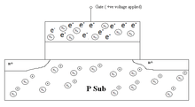
Vgs = Gate Voltage
'Vth = Threshold Voltage
n+ = Highly doped N region
In figure 1(a) it is observed that the free majority carriers are scattered throughout the structure because of the absence of an external electric field. When a positive field is applied on the gate, the scattered carriers arrange themselves like figure 1(b), the electrons move closer toward the gate terminal but due to the open circuit configuration they don't start to flow. As a result of the separation of charges a depletion region is formed on the polysilicon-oxide interface, which has a direct effect on the channel formation in MOSFETs.[2]
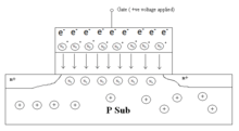
In an NMOS with n+ Polysilicon gate, the poly depletion effect aids in the channel formation by the combined effect of the (+)ve field of donor ions (ND) and the externally applied (+)ve field at gate terminal. Basically the accumulation of the (+)ve charged Donor ions (ND) on the polysilicon enhances the Formation of the inversion channel and when Vgs > Vth an inversion layer is formed, which can be seen in the figure 1(b) where the inversion channel is formed of acceptor ions (NA) (minority carriers).[3] Polysilicon depletion can vary laterally across a transistor depending on the fabrication process, which can lead to significant transistor variability in certain transistor dimensions.[4]
Metal gate contacts re-introduced
For the above reason as the devices go down on the scaling (32-28nm nodes) poly gates are being replaced by metal gates. The following technology is known as High-k Dielectric Metal Gate (HKMG) integration.[5] Recently, Intel also released a press-kit regarding their fabrication procedures of different nodes, which showed the use of Metal gate technology.[6]
Doped polysilicon was preferred earlier as gate material in MOS devices. Polysilicons were used as their work function matched with the Si substrate (which results in the low threshold voltage of MOSFET). Metal gates were re-introduced at the time when SiO2 dielectrics are being replaced by high-k dielectrics like Hafnium oxide as gate oxide in the mainstream CMOS technology.[7] Also at the interface with gate dielectric, Polysilicon forms an SiOx layer. Moreover, there remains a high probability for Fermi level pinning to occur.[8] So the effect with doped poly is an undesired reduction of threshold voltage that wasn't taken into account during circuit simulation. In order to avoid this kind of variation in vth of the MOSFET, at present metal gate is preferred over Polysilicon.
See also
References
- Rios, R.; Arora, N.D. (1994). "An analytic polysilicon depletion effect model for MOSFETs". IEEE Electron Device Letters. 15 (4): 129–131. doi:10.1109/55.285407.
- Rios, R.; Arora, N.D. (1994). "Modeling the polysilicon depletion effect and its impact on submicrometer CMOS circuit performance". IEEE Transactions on Electron Devices. 42 (5): 935–943. doi:10.1109/16.381991.
- Schuegraf, K.F.; King, C.C.; Hu, C. (1993). "Impact of polysilicon depletion in thin oxide MOS technology" (PDF). Proceedings International Symposium: VLSI Technology Systems and Applications. pp. 86–90.
- H. P. Tuinhout, A. H. Montree, J. Schmitz and P. A. Stolk, Effects of gate depletion and boron penetration on matching of deep submicron CMOS transistors, IEEE International Electron Device Meeting, Technical Digest pp. 631-634, 1997.
- Global Foundries
- "From Sand to Silicon: The Making of Chip" (Press release). Intel Technology. Nov 11, 2011. Retrieved 2013-06-08.
- Chau, Robert (Nov 6, 2003). "Gate Dielectric Scaling for CMOS: from SiO2/PolySi to High-K/Metal-Gate" (White paper) (Press release). Intel Technology. Retrieved 2013-06-08.
- Hobbs, C.C.; Fonseca, L. R. C.; Knizhnik, A. (2004). "Fermi-level pinning at the polysilicon/metal oxide interface-Part I". IEEE Transactions on Electron Devices. 51 (6): 971–977. doi:10.1109/TED.2004.829513.