Wright etch
The Wright Etch is a preferential etch for revealing defects in <100> and <111> oriented, p- and n-type silicon. It was developed by Margaret Wright Jenkins in 1976 while working in research and development at Motorola Inc. It was published in 1977.[1] This etchant reveals clearly defined oxidation-induced stacking faults, dislocations, swirls and striations with minimum surface roughness or extraneous pitting. These defects are known causes of shorts and current leakage in finished semiconductor devices (such as transistors) should they fall across isolated junctions. A relatively low etch rate (~1 micrometre per minute) at room temperature provides etch control. The long shelf life of this etchant allows the solution to be stored in large quantities. The present report summarizes the highlights of the Wright etch. For a detailed discussion of observation and findings, please consult the original article. [1]
Etch formula
The composition of the Wright etch is as follows:
60 ml conc. HF (hydrofluoric acid)
30 ml conc. HNO3 (nitric acid)
30 ml of 5 mole CrO3 (mix 1 gram of chromium trioxide per 2 ml of water; the numbers are suspiciously round because the molecular weight of chromium trioxide is almost exactly 100)
2 grams Cu (NO3)2 . 3H2O (Copper II Nitrate Trihydrate )
60 ml conc. CH3COOH (acetic acid)
60 ml H2O (deionized water)
In mixing the solution, the best results are obtained by first dissolving the copper nitrate in the given amount of water; otherwise the order of mixing is not critical.
Etch mechanism
The Wright etch consistently produces well-defined etch figures of common defects on silicon surfaces. This attribute is attributed to the interactions of the selected chemicals in the formula. Robbins and Schwartz [2][3][4] described chemical etching of silicon in detail using an HF, HNO3 and H2O system; and an HF, HNO3, H2O and CH3COOH (acetic acid) system. Briefly, the etching of silicon is a two-step process. First, the top surface of the silicon is converted into a soluble oxide by a suitable oxidizing agent(s). Then the resulting oxide layer is removed from the surface by dissolution in a suitable solvent, usually HF. This is a continuous process during the etch cycle. In order to delineate a crystal defect, the defect area must be oxidized at a slower or faster rate than the surrounding area thereby forming a mound or pit during the preferential etch process.
In the present system, the silicon is oxidized with HNO3, CrO3 solution (which in this case contains the Cr2O72− dichromate ion, since the pH is low - see the phase diagram in Chromic acid) and Cu (NO3)2. The dichromate ion, a strong oxidizing agent, is considered to be the principal oxidizing agent. The ratio of HNO3 to CrO3 solution stated in the formula produces a superior etched surface. Other ratios produce less desirable finishes. With the addition of a small amount of Cu (NO3)2, the definition of the defect was enhanced. Therefore, it is believed that the Cu (NO3)2 affects the localized differential oxidation rate at the defect site. The addition of the acetic acid gave the background surface of the etched silicon a smooth finish. It is theorized that this effect is attributed to the wetting action of the acetic acid which prevents the formation of bubbles during etching.
All experimental preferential etching to show defects was done on cleaned and oxidized wafers. All oxidations were performed at 1200º C in steam for 75 minutes. Fig. 1(a) shows oxidation-induced stacking faults in <100> oriented wafers after 30 minutes Wright etch, (b) and (c) show dislocation pits on <100> and <111> oriented wafers respectively after 20 minutes Wright Etch.
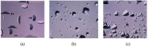
Fig1 (a). Oxidation-induced stacking faults on a <100> , 7-10 Ω-cm, boron-doped wafer after 30 min Wright etch (the A arrow in this figure points to the shape of faults that intersect the surface, while B points to bulk faults), (b) and (c) show dislocation pits on <100> and <111> oriented wafers respectively after 20 min Wright etch.
Summary
This etch process is a quick and reliable method of determining the integrity of pre-processed polished silicon wafers or to reveal defects that may be induced at any point during wafer processing. It has been demonstrated that Wright etch is superior in revealing stacking faults and dislocation etch figures when compared with those revealed by Sirtl [5] and Secco [6] etchings. Please see comparison micrographs below. This etch is widely used in failure analysis of electrical devices at various wafer processing stages as seen in articles: "Pipeline Defects in Flash Devices Associated with Rings OSF" * and "Defect Etching in Silicon" * . In these publications, by comparison, the Wright etch was the preferred etchant to reveal defects in silicon crystals.
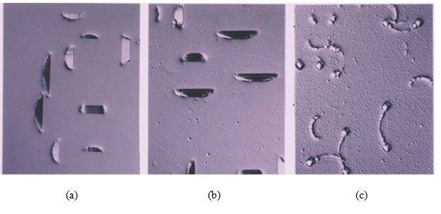
Figure 2 shows a comparison of oxidation -induced stacking fault delineation on <100> oriented wafers after Wright etch, Secco and Sirtl etch respectively. Figure 3 shows a comparison of dislocation pits delineation on <100> oriented wafers after Wright etch, Secco and Sirtl etch. The final fig 4, shows a comparison of dislocation pits revealed on <111> oriented wafer after etching with Wright etch, Secco and Sirtl etch respectively.
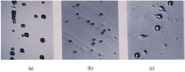
Fig. 3. A comparison of dislocation delineation on a <100> oriented, 10-20 Ω-cm, boron doped wafer after oxidation and preferential etching. (a) After 20 min Wright etch, (b) 10 min Secco etch and (c) 6 min Sirtl etch.
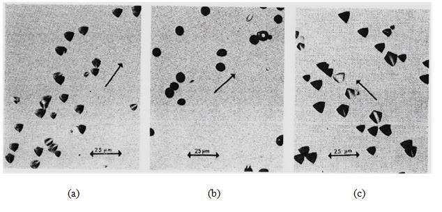
Fig. 4. A comparison of dislocation delineation on a <111> oriented, 10-20 Ω-cm, boron-doped wafer after oxidation and preferential etching. (a) After 10 min Wright etch, (b) 10 min Secco etch and (c) 3 min Sirtl etch. The arrows indicate slip direction.
Note: Please be environmentally responsible when disposing of spent chemicals.
References
- 1 2 Margaret Wright Jenkins. (1977). Journal of the Electrochemical Society. 124 (5): 757–759
- ↑ Robbins, H.; Schwartz, B. (1959). Journal of The Electrochemical Society. 106 (6): 505–508
- ↑ Robbins, H.; Schwartz, B. (1960). Journal of The Electrochemical Society. 107 (2): 108–111
- ↑ Robbins, H.; Schwartz, B. (1961). Journal of The Electrochemical Society. 108 (4): 365–372
- ↑ Sirtl, E.; Adler. A. (1961). Zeitschrift für Metallkunde. 52: 529–534
- ↑ Secco d'Aragona, F. (1972). Journal of The Electrochemical Society. 119 (7): 948–951
External links
- https://wright-etch.blogspot.com/ A static copy of the 1977 original publication
- http://www.tf.uni-kiel.de/matwis/amat/def_en/kap_6/advanced/t6_1_2.html