RSX Reality Synthesizer
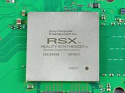
The RSX 'Reality Synthesizer' is a proprietary graphics processing unit (GPU) codeveloped by Nvidia and Sony for the PlayStation 3 game console. It is a GPU based on the Nvidia 7800GTX graphics processor and, according to Nvidia, is a G70/G71 (previously known as NV47) hybrid architecture with some modifications. The RSX has separate vertex and pixel shader pipelines. The GPU makes use of 256 MB GDDR3 RAM clocked at 650 MHz with an effective transmission rate of 1.4 GHz and up to 224 MB of the 3.2 GHz XDR main memory via the CPU (480 MB max). Although it carries the majority of the graphics processing, the Cell Broadband Engine, the console's CPU, is also used complementarily for some graphics-related computational loads of the console.
Specifications

Unless otherwise noted, the following specifications are based on a press release by Sony at the E3 2005 conference,[1] slides from the same conference,[2] and slides from a Sony presentation at the 2006 Game Developer's Conference.
- 500 MHz on 90 nm process (shrunk to 65 nm in 2008[3] and to 40 nm in 2010[4]), 300+ million transistors
- Based on NV47 (Nvidia GeForce 7800 architecture)
- Little Endian
- Multi-way programmable parallel floating-point shader pipelines, independent pixel/vertex shader architecture
- 24 parallel pixel-shader ALU pipelines clocked at 550 MHz
- 8 parallel vertex pipelines
- 2 ALU operations per pipeline, per cycle (1 vector4 and 1 scalar, dual issue)
- 10 FLOPS per pipeline, per cycle[7]
- 24 texture filtering units (TF) and 8 vertex texture addressing units (TA)
- 24 filtered samples per clock
- Maximum Texel fillrate: 12.0 Gigatexels per second (24 textures * 500 MHz)
- 32 unfiltered texture samples per clock (8 TA * 4 texture samples)
- 8 render output units (ROPs) / pixel rendering pipelines
- Peak pixel fillrate (theoretical): 4.0 Gigapixel per second
- Maximum Z-buffering sample rate: 8.0 Gigasamples per second (2 Z-samples * 8 ROPs * 500 MHz)
- Maximum dot product operations: 51 billion per second (combined with Cell CPU)
- 128-bit pixel precision offers High Dynamic Range rendering
- 256 MB GDDR3 RAM at 650 MHz
- 128-bit memory bus width
- 22.4 GB/s read and write bandwidth
- Cell FlexIO bus interface
- Rambus XDR Memory interface bus width: 56bit out of 64bit (serial)
- 20 GB/s read to the Cell and XDR memory
- 15 GB/s write to the Cell and XDR memory
- 576 KB texture cache (96 KB per quad of pixel pipelines)
- Support for PSGL (OpenGL ES 1.1 + Nvidia Cg)
- Support for S3 Texture Compression[8]
Other features: Support for Bilinear, trilinear, anisotropic, quincunx texture filtering, quincunx antialiasing, up to 4xMSAA, SSAA, Alpha to Coverage and Alphakill.
Model numbers
90nm:
- CXD2971AGB
- CXD2971DGB
- CXD2971GB
- CXD2971-1GB
- CXD297BGB
65nm:
- CXD2982
- CXD2982GB
- CXD2991GB
- CXD2991BGB
- CXD2991GGB
- CXD2991CGB
- CXD2991EGB
40nm:
- CXD5300AGB
- CXD5300A1GB
- CXD5301DGB
- CXD5302DGB
- CXD5302A1GB
Local GDDR3 physical memory structure
- Total Memory 256MB
- 2 Partitions (128MB)
- 64bit bus per partition
- 8 Banks per partition (16MB)
- 4096 Pages per bank (4KB) -> 12bit Row Address
- Memory block in a page -> 9bit Column Address
- Minimum access granularity = 8 bytes -> same as buswidth between RSX <> GDDR
RSX memory map
Although the RSX has 256MB of GDDR3 RAM, not all of it is usable. The last 4MB is reserved for keeping track of the RSX internal state and issued commands. The 4MB of GPU Data contains RAMIN, RAMHT, RAMFC, DMA Objects, Graphic Objects, and the Graphic Context. The following is a breakdown of the address within 256MB of the RSX.
| Address Range | Size | Comment |
|---|---|---|
| 0000000-FBFFFFF | 252 MB | Framebuffer |
| FC00000-FFFFFFF | 4 MB | GPU Data |
| FF80000-FFFFFFF | 512KB | RAMIN: Instance Memory |
| FF90000-FF93FFF | 16KB | RAMHT: Hash Table |
| FFA0000-FFA0FFF | 4KB | RAMFC: FIFO Context |
| FFC0000-FFCFFFF | 64KB | DMA Objects |
| FFD0000-FFDFFFF | 64KB | Graphic Objects |
| FFE0000-FFFFFFF | 128KB | GRAPH: Graphic Context |
Besides local GDDR3 memory, main XDR memory can be accessed by RSX too, which is limited to either:
- 0MB - 256MB (0x00000000 - 0x0FFFFFFF)
- -or-
- 0MB - 512MB (0x00000000 - 0x1FFFFFFF)
Speed, bandwidth and latency
System bandwidth (theoretical maximum):
- Cell to/from 256MB XDR : 25.6 GB/s
- Cell to RSX (IOIFO): 20GB/s (practical : 15.8GB/s @ packetsize 128B)
- Cell from RSX (IOIFI) : 15GB/s (practical : 11.9GB/s @ packetsize 128B)
- RSX to/from 256MB GDDR3 : 20.8GB/s (@ 650 MHz)
Because of the aforementioned layout of the communication path between the different chips, and the latency and bandwidth differences between the various components, there are different access speeds depending on the direction of the access in relation to the source and destination. The following is a chart showing the speed of reads and writes to the GDDR3 and XDR memory from the viewpoint of the Cell and RSX. Note that these are measured speeds (rather than calculated speeds) and they should be worse if RSX and GDDR3 access are involved because these figures were measured when the RSX was clocked at 550Mhz and the GDDR3 memory was clocked at 700Mhz. The shipped PS3 has the RSX clocked in at 500Mhz (front and back end, although the pixel shaders run separately inside at 550Mhz). In addition, the GDDR3 memory was also clocked lower at 650Mhz.
Speed table
| Processor | 256MB XDR | 256MB GDDR3 |
|---|---|---|
| Cell Read | 16.8GB/s | 16MB/s (15.6MB/s @ 650 MHz) |
| Cell Write | 24.9GB/s | 4GB/s |
| RSX Read | 15.5GB/s | 22.4GB/s (20.8GB/s @ 650 MHz) |
| RSX Write | 10.6GB/s | 22.4GB/s (20.8GB/s @ 650 MHz) |
Because of the very slow Cell Read speed from the 256MB GDDR3 memory, it is more efficient for the Cell to work in XDR and then have the RSX pull data from XDR and write to GDDR3 for output to the HDMI display. This is why extra texture lookup instructions were included in the RSX to allow loading data from XDR memory (as opposed to the local GDDR3 memory).
RSX libraries
The RSX is dedicated to 3D graphics, and developers are able to use different API libraries to access its features. The easiest way is to use high level PSGL, which is basicially OpenGL|ES with programmable pipeline added in, however this is unpopular due to the performance overhead on a relatively weak console CPU. At a lower level developers can use LibGCM, which is an API that builds RSX command buffers at a lower level. (PSGL is actually implemented on top of LibGCM). This is done by setting up commands (via FIFO Context) and DMA Objects and issuing them to the RSX via DMA calls.
Differences with the G70 architecture
The RSX 'Reality Synthesizer' is based on the G70 architecture, but features a few changes to the core.[9] The biggest difference between the two chips is the way the memory bandwidth works. The G70 only supports rendering to local memory, while the RSX is able to render to both system and local memory. Since rendering from system memory has a much higher latency compared to rendering from local memory, the chip's architecture had to be modified to avoid a performance penalty. This was achieved by enlarging the chip size to accommodate larger buffers and caches in order to keep the graphics pipeline full. The result was that the RSX only has 60% of the local memory bandwidth of the G70, making it necessary for developers to use the system memory in order to achieve performance targets.[9]
| Difference | RSX | nVidia 7800GTX |
|---|---|---|
| GDDR3 Memory bus | 128bit | 256bit |
| ROPs | 8 | 16 |
| Post Transform and Lighting Cache | 63 max vertices | 45 max vertices |
| Total Texture Cache Per Quad of Pixel Pipes (L1 and L2) | 96kB | 48kB |
| CPU interface | FlexIO | PCI-Express 16x |
| Technology | 40 nm/65 nm/90 nm | 110 nm |
Other RSX features/differences include:
- More shader instructions
- Extra texture lookup logic (helps RSX transport data from XDR)
- Fast vector normalize
Press releases
Sony staff were quoted in PlayStation Magazine saying that the "RSX shares a lot of inner workings with NVIDIA 7800 which is based on G70 architecture." Since the G70 is capable of carrying out 136 shader operations per clock cycle, the RSX was expected to feature the same number of parallel pixel and vertex shader pipelines as the G70, which contains 24 pixel and 8 vertex pipelines.
Nvidia CEO Jen-Hsun Huang stated during Sony's pre-show press conference at E3 2005 that the RSX is twice as powerful as the GeForce 6800 Ultra.[2]
See also
- Xenos - GPU used in the Xbox 360
- Cell Broadband Engine - CPU used in the PlayStation 3
References
- ↑ "SONY COMPUTER ENTERTAINMENT INC. TO LAUNCH ITS NEXT GENERATION COMPUTER ENTERTAINMENT SYSTEM, PLAYSTATION3 IN SPRING 2006" (Press release). Sony Computer Entertainment Inc. 2005-05-16.
- 1 2 "Sony Introduces PlayStation 3, to launch in 2006". AnandTech. 2005-05-16.
- ↑ "PS3 Graphics Chip Goes 65nm in Fall". Edge Online. 2008-06-26.
- ↑ "Sony PS3 upgraded with cooler 40-nm RSX graphics chip, profits await (updated)". Engadget. 2010-04-26.
- ↑ Ryan Shrout (June 22, 2005). "NVIDIA GeForce 7800 GTX GPU Review".
- ↑ "Nvidia Corp Tegra K1 Whitepaper" (PDF).
- ↑ Computing (2005-06-22). "Page 3 - GeForce 7800 GTX: Nvidia's Nuclear Option". ExtremeTech. Retrieved 2013-06-25.
- ↑ Gantayat, Anoop (2006-01-30). "New PS3 tools". IGN.com. Retrieved 2006-08-28.
- 1 2 "Microsoft's Xbox 360, Sony's PS3 - A Hardware Discussion". Retrieved 2014-03-08.