Solar cell


A solar cell, or photovoltaic cell, is an electrical device that converts the energy of light directly into electricity by the photovoltaic effect, which is a physical and chemical phenomenon.[1] It is a form of photoelectric cell, defined as a device whose electrical characteristics, such as current, voltage, or resistance, vary when exposed to light. Individual solar cell devices can be combined to form modules, otherwise known as solar panels. In basic terms a single junction silicon solar cell can produce a maximum open-circuit voltage of approximately 0.5 to 0.6 volts.[2]
Solar cells are described as being photovoltaic, irrespective of whether the source is sunlight or an artificial light. They are used as a photodetector (for example infrared detectors), detecting light or other electromagnetic radiation near the visible range, or measuring light intensity.
The operation of a photovoltaic (PV) cell requires three basic attributes:
- The absorption of light, generating either electron-hole pairs or excitons.
- The separation of charge carriers of opposite types.
- The separate extraction of those carriers to an external circuit.
In contrast, a solar thermal collector supplies heat by absorbing sunlight, for the purpose of either direct heating or indirect electrical power generation from heat. A "photoelectrolytic cell" (photoelectrochemical cell), on the other hand, refers either to a type of photovoltaic cell (like that developed by Edmond Becquerel and modern dye-sensitized solar cells), or to a device that splits water directly into hydrogen and oxygen using only solar illumination.
Applications
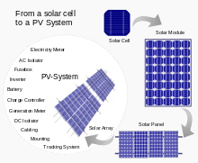
Assemblies of solar cells are used to make solar modules that generate electrical power from sunlight, as distinguished from a "solar thermal module" or "solar hot water panel". A solar array generates solar power using solar energy.
Cells, modules, panels and systems
Multiple solar cells in an integrated group, all oriented in one plane, constitute a solar photovoltaic panel or module. Photovoltaic modules often have a sheet of glass on the sun-facing side, allowing light to pass while protecting the semiconductor wafers. Solar cells are usually connected in series and parallel circuits or series in modules, creating an additive voltage. Connecting cells in parallel yields a higher current; however, problems such as shadow effects can shut down the weaker (less illuminated) parallel string (a number of series connected cells) causing substantial power loss and possible damage because of the reverse bias applied to the shadowed cells by their illuminated partners. Strings of series cells are usually handled independently and not connected in parallel, though as of 2014, individual power boxes are often supplied for each module, and are connected in parallel. Although modules can be interconnected to create an array with the desired peak DC voltage and loading current capacity, using independent MPPTs (maximum power point trackers) is preferable. Otherwise, shunt diodes can reduce shadowing power loss in arrays with series/parallel connected cells.
| USD/W | Australia | China | France | Germany | Italy | Japan | United Kingdom | United States |
|---|---|---|---|---|---|---|---|---|
| Residential | 1.8 | 1.5 | 4.1 | 2.4 | 2.8 | 4.2 | 2.8 | 4.9 |
| Commercial | 1.7 | 1.4 | 2.7 | 1.8 | 1.9 | 3.6 | 2.4 | 4.5 |
| Utility-scale | 2.0 | 1.4 | 2.2 | 1.4 | 1.5 | 2.9 | 1.9 | 3.3 |
| Source: IEA – Technology Roadmap: Solar Photovoltaic Energy report, 2014 edition[3]:15 Note: DOE – Photovoltaic System Pricing Trends reports lower prices for the U.S.[4] | ||||||||
History
The photovoltaic effect was experimentally demonstrated first by French physicist Edmond Becquerel. In 1839, at age 19, he built the world's first photovoltaic cell in his father's laboratory. Willoughby Smith first described the "Effect of Light on Selenium during the passage of an Electric Current" in a 20 February 1873 issue of Nature. In 1883 Charles Fritts built the first solid state photovoltaic cell by coating the semiconductor selenium with a thin layer of gold to form the junctions; the device was only around 1% efficient.
In 1888 Russian physicist Aleksandr Stoletov built the first cell based on the outer photoelectric effect discovered by Heinrich Hertz in 1887.[5]
In 1905 Albert Einstein proposed a new quantum theory of light and explained the photoelectric effect in a landmark paper, for which he received the Nobel Prize in Physics in 1921.[6]
Vadim Lashkaryov discovered p-n-junctions in Cu O and silver sulphide protocells in 1941.[7]

Russell Ohl patented the modern junction semiconductor solar cell in 1946[8] while working on the series of advances that would lead to the transistor.
The first practical photovoltaic cell was publicly demonstrated on 25 April 1954 at Bell Laboratories.[9] The inventors were Calvin Souther Fuller, Daryl Chapin and Gerald Pearson.[10]
Solar cells gained prominence with their incorporation onto the 1958 Vanguard I satellite.
Space applications
Solar cells were first used in a prominent application when they were proposed and flown on the Vanguard satellite in 1958, as an alternative power source to the primary battery power source. By adding cells to the outside of the body, the mission time could be extended with no major changes to the spacecraft or its power systems. In 1959 the United States launched Explorer 6, featuring large wing-shaped solar arrays, which became a common feature in satellites. These arrays consisted of 9600 Hoffman solar cells.
By the 1960s, solar cells were (and still are) the main power source for most Earth orbiting satellites and a number of probes into the solar system, since they offered the best power-to-weight ratio. However, this success was possible because in the space application, power system costs could be high, because space users had few other power options, and were willing to pay for the best possible cells. The space power market drove the development of higher efficiencies in solar cells up until the National Science Foundation "Research Applied to National Needs" program began to push development of solar cells for terrestrial applications.
In the early 1990s the technology used for space solar cells diverged from the silicon technology used for terrestrial panels, with the spacecraft application shifting to gallium arsenide-based III-V semiconductor materials, which then evolved into the modern III-V multijunction photovoltaic cell used on spacecraft.
Price reductions
Improvements were gradual over the 1960s. This was also the reason that costs remained high, because space users were willing to pay for the best possible cells, leaving no reason to invest in lower-cost, less-efficient solutions. The price was determined largely by the semiconductor industry; their move to integrated circuits in the 1960s led to the availability of larger boules at lower relative prices. As their price fell, the price of the resulting cells did as well. These effects lowered 1971 cell costs to some $100 per watt.[11]
In late 1969 Elliot Berman joined Exxon's task force which was looking for projects 30 years in the future and in April 1973 he founded Solar Power Corporation, a wholly owned subsidiary of Exxon at that time.[12][13][14] The group had concluded that electrical power would be much more expensive by 2000, and felt that this increase in price would make alternative energy sources more attractive. He conducted a market study and concluded that a price per watt of about $20/watt would create significant demand.[12] The team eliminated the steps of polishing the wafers and coating them with an anti-reflective layer, relying on the rough-sawn wafer surface. The team also replaced the expensive materials and hand wiring used in space applications with a printed circuit board on the back, acrylic plastic on the front, and silicone glue between the two, "potting" the cells.[15] Solar cells could be made using cast-off material from the electronics market. By 1973 they announced a product, and SPC convinced Tideland Signal to use its panels to power navigational buoys, initially for the U.S. Coast Guard.[13]
Research and industrial production
Research into solar power for terrestrial applications became prominent with the U.S. National Science Foundation's Advanced Solar Energy Research and Development Division within the "Research Applied to National Needs" program, which ran from 1969 to 1977,[16] and funded research on developing solar power for ground electrical power systems. A 1973 conference, the "Cherry Hill Conference", set forth the technology goals required to achieve this goal and outlined an ambitious project for achieving them, kicking off an applied research program that would be ongoing for several decades.[17] The program was eventually taken over by the Energy Research and Development Administration (ERDA),[18] which was later merged into the U.S. Department of Energy.
Following the 1973 oil crisis, oil companies used their higher profits to start (or buy) solar firms, and were for decades the largest producers. Exxon, ARCO, Shell, Amoco (later purchased by BP) and Mobil all had major solar divisions during the 1970s and 1980s. Technology companies also participated, including General Electric, Motorola, IBM, Tyco and RCA.[19]
Declining costs and exponential growth
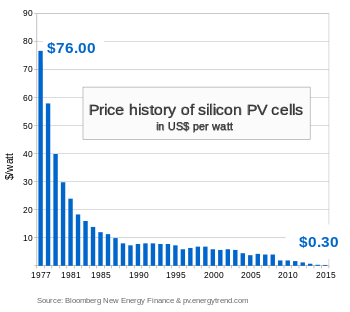

Adjusting for inflation, it cost $96 per watt for a solar module in the mid-1970s. Process improvements and a very large boost in production have brought that figure down 99%, to 68¢ per watt in 2016, according to data from Bloomberg New Energy Finance.[20] Swanson's law is an observation similar to Moore's Law that states that solar cell prices fall 20% for every doubling of industry capacity. It was featured in an article in the British weekly newspaper The Economist in late 2012.[21]
Further improvements reduced production cost to under $1 per watt, with wholesale costs well under $2. Balance of system costs were then higher than those of the panels. Large commercial arrays could be built, as of 2010, at below $3.40 a watt, fully commissioned.[22][23]
As the semiconductor industry moved to ever-larger boules, older equipment became inexpensive. Cell sizes grew as equipment became available on the surplus market; ARCO Solar's original panels used cells 2 to 4 inches (50 to 100 mm) in diameter. Panels in the 1990s and early 2000s generally used 125 mm wafers; since 2008, almost all new panels use 156 mm cells. The widespread introduction of flat screen televisions in the late 1990s and early 2000s led to the wide availability of large, high-quality glass sheets to cover the panels.
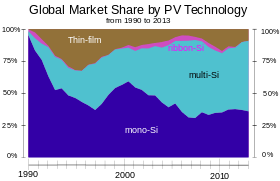
During the 1990s, polysilicon ("poly") cells became increasingly popular. These cells offer less efficiency than their monosilicon ("mono") counterparts, but they are grown in large vats that reduce cost. By the mid-2000s, poly was dominant in the low-cost panel market, but more recently the mono returned to widespread use.
Manufacturers of wafer-based cells responded to high silicon prices in 2004–2008 with rapid reductions in silicon consumption. In 2008, according to Jef Poortmans, director of IMEC's organic and solar department, current cells use 8–9 grams (0.28–0.32 oz) of silicon per watt of power generation, with wafer thicknesses in the neighborhood of 200 microns. Crystalline silicon panels dominate worldwide markets and are mostly manufactured in China and Taiwan. By late 2011, a drop in European demand dropped prices for crystalline solar modules to about $1.09[23] per watt down sharply from 2010. Prices continued to fall in 2012, reaching $0.62/watt by 4Q2012.[24]
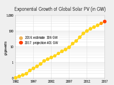
Solar PV is growing fastest in Asia, with China and Japan currently accounting for half of worldwide deployment.[25] Global installed PV capacity reached at least 301 gigawatts in 2016, and grew to supply 1.3% of global power by 2016.[26]

In fact, the harnessed energy of silicon solar cells at the cost of a dollar has surpassed its oil counterpart since 2004.[27] It was anticipated that electricity from PV will be competitive with wholesale electricity costs all across Europe and the energy payback time of crystalline silicon modules can be reduced to below 0.5 years by 2020.[28]
Subsidies and grid parity
Solar-specific feed-in tariffs vary by country and within countries. Such tariffs encourage the development of solar power projects. Widespread grid parity, the point at which photovoltaic electricity is equal to or cheaper than grid power without subsidies, likely requires advances on all three fronts. Proponents of solar hope to achieve grid parity first in areas with abundant sun and high electricity costs such as in California and Japan.[29] In 2007 BP claimed grid parity for Hawaii and other islands that otherwise use diesel fuel to produce electricity. George W. Bush set 2015 as the date for grid parity in the US.[30][31] The Photovoltaic Association reported in 2012 that Australia had reached grid parity (ignoring feed in tariffs).[32]
The price of solar panels fell steadily for 40 years, interrupted in 2004 when high subsidies in Germany drastically increased demand there and greatly increased the price of purified silicon (which is used in computer chips as well as solar panels). The recession of 2008 and the onset of Chinese manufacturing caused prices to resume their decline. In the four years after January 2008 prices for solar modules in Germany dropped from €3 to €1 per peak watt. During that same time production capacity surged with an annual growth of more than 50%. China increased market share from 8% in 2008 to over 55% in the last quarter of 2010.[33] In December 2012 the price of Chinese solar panels had dropped to $0.60/Wp (crystalline modules).[34] (The abbreviation Wp stands for watt peak capacity, or the maximum capacity under optimal conditions.[35])
As of the end of 2016, it was reported that spot prices for assembled solar panels (not cells) had fallen to a record-low of US$0.36/Wp. It was estimated that the world's largest producer, Trina Solar Ltd. of China, was probably selling at a loss. The second largest supplier, Canadian Solar Inc., had reported costs of US$0.37/Wp in the third quarter of 2016, having dropped $0.02 from the previous quarter, and hence was probably still at least breaking even. Many producers expected costs would drop to the vicinity of $0.30 by the end of 2017.[36] It was also reported that new solar installations were cheaper than coal-based thermal power plants in some regions of the world, and this was expected to be the case in most of the world within a decade.[37]
Theory

The solar cell works in several steps:
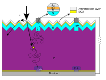
- Photons in sunlight hit the solar panel and are absorbed by semiconducting materials, such as silicon.
- Electrons are excited from their current molecular/atomic orbital. Once excited an electron can either dissipate the energy as heat and return to its orbital or travel through the cell until it reaches an electrode. Current flows through the material to cancel the potential and this electricity is captured. The chemical bonds of the material are vital for this process to work, and usually silicon is used in two layers, one layer being doped with boron, the other phosphorus. These layers have different chemical electric charges and subsequently both drive and direct the current of electrons.[1]
- An array of solar cells converts solar energy into a usable amount of direct current (DC) electricity.
- An inverter can convert the power to alternating current (AC).
The most commonly known solar cell is configured as a large-area p–n junction made from silicon. Other possible solar cell types are organic solar cells, dye sensitized solar cells, perovskite solar cells, quantum dot solar cells etc. The illuminated side of a solar cell generally have a transparent conducting film for allowing light to enter into active material and to collect the generated charge carriers. Typically, films with high transmittance and high electrical conductance such as indium tin oxide, conducting polymers or conducting nanowire networks are used for the purpose.[38]
Efficiency

Solar cell efficiency may be broken down into reflectance efficiency, thermodynamic efficiency, charge carrier separation efficiency and conductive efficiency. The overall efficiency is the product of these individual metrics.
The power conversion efficiency of a solar cell is a parameter which is defined by the fraction of incident power converted into electricity.[39]
A solar cell has a voltage dependent efficiency curve, temperature coefficients, and allowable shadow angles.
Due to the difficulty in measuring these parameters directly, other parameters are substituted: thermodynamic efficiency, quantum efficiency, integrated quantum efficiency, VOC ratio, and fill factor. Reflectance losses are a portion of quantum efficiency under "external quantum efficiency". Recombination losses make up another portion of quantum efficiency, VOC ratio, and fill factor. Resistive losses are predominantly categorized under fill factor, but also make up minor portions of quantum efficiency, VOC ratio.
The fill factor is the ratio of the actual maximum obtainable power to the product of the open circuit voltage and short circuit current. This is a key parameter in evaluating performance. In 2009, typical commercial solar cells had a fill factor > 0.70. Grade B cells were usually between 0.4 and 0.7.[40] Cells with a high fill factor have a low equivalent series resistance and a high equivalent shunt resistance, so less of the current produced by the cell is dissipated in internal losses.
Single p–n junction crystalline silicon devices are now approaching the theoretical limiting power efficiency of 33.16%,[41] noted as the Shockley–Queisser limit in 1961. In the extreme, with an infinite number of layers, the corresponding limit is 86% using concentrated sunlight.[42]
In 2014, three companies broke the record of 25.6% for a silicon solar cell. Panasonic's was the most efficient. The company moved the front contacts to the rear of the panel, eliminating shaded areas. In addition they applied thin silicon films to the (high quality silicon) wafer's front and back to eliminate defects at or near the wafer surface.[43]
In 2015, a 4-junction GaInP/GaAs//GaInAsP/GaInAs solar cell achieved a new laboratory record efficiency of 46.1 percent (concentration ratio of sunlight = 312) in a French-German collaboration between the Fraunhofer Institute for Solar Energy Systems (Fraunhofer ISE), CEA-LETI and SOITEC.[44]
In September 2015, Fraunhofer ISE announced the achievement of an efficiency above 20% for epitaxial wafer cells. The work on optimizing the atmospheric-pressure chemical vapor deposition (APCVD) in-line production chain was done in collaboration with NexWafe GmbH, a company spun off from Fraunhofer ISE to commercialize production.[45][46]
For triple-junction thin-film solar cells, the world record is 13.6%, set in June 2015.[47]
In 2016, researchers at Fraunhofer ISE announced a GaInP/GaAs/Si triple-junction solar cell with two terminals reaching 30.2% efficiency without concentration.[48]
In 2017, a team of researchers at National Renewable Energy Laboratory (NREL), EPFL and CSEM (Switzerland) reported record one-sun efficiencies of 32.8% for dual-junction GaInP/GaAs solar cell devices. In addition, the dual-junction device was mechanically stacked with a Si solar cell, to achieve a record one-sun efficiency of 35.9% for triple-junction solar cells.[49]
a.jpg)
Materials
Solar cells are typically named after the semiconducting material they are made of. These materials must have certain characteristics in order to absorb sunlight. Some cells are designed to handle sunlight that reaches the Earth's surface, while others are optimized for use in space. Solar cells can be made of only one single layer of light-absorbing material (single-junction) or use multiple physical configurations (multi-junctions) to take advantage of various absorption and charge separation mechanisms.
Solar cells can be classified into first, second and third generation cells. The first generation cells—also called conventional, traditional or wafer-based cells—are made of crystalline silicon, the commercially predominant PV technology, that includes materials such as polysilicon and monocrystalline silicon. Second generation cells are thin film solar cells, that include amorphous silicon, CdTe and CIGS cells and are commercially significant in utility-scale photovoltaic power stations, building integrated photovoltaics or in small stand-alone power system. The third generation of solar cells includes a number of thin-film technologies often described as emerging photovoltaics—most of them have not yet been commercially applied and are still in the research or development phase. Many use organic materials, often organometallic compounds as well as inorganic substances. Despite the fact that their efficiencies had been low and the stability of the absorber material was often too short for commercial applications, there is a lot of research invested into these technologies as they promise to achieve the goal of producing low-cost, high-efficiency solar cells.
Crystalline silicon
By far, the most prevalent bulk material for solar cells is crystalline silicon (c-Si), also known as "solar grade silicon". Bulk silicon is separated into multiple categories according to crystallinity and crystal size in the resulting ingot, ribbon or wafer. These cells are entirely based around the concept of a p-n junction. Solar cells made of c-Si are made from wafers between 160 and 240 micrometers thick.
Monocrystalline silicon
Monocrystalline silicon (mono-Si) solar cells are more efficient and more expensive than most other types of cells. The corners of the cells look clipped, like an octagon, because the wafer material is cut from cylindrical ingots, that are typically grown by the Czochralski process. Solar panels using mono-Si cells display a distinctive pattern of small white diamonds.
Epitaxial silicon development
Epitaxial wafers of crystalline silicon can be grown on a monocrystalline silicon "seed" wafer by chemical vapor deposition (CVD), and then detached as self-supporting wafers of some standard thickness (e.g., 250 µm) that can be manipulated by hand, and directly substituted for wafer cells cut from monocrystalline silicon ingots. Solar cells made with this "kerfless" technique can have efficiencies approaching those of wafer-cut cells, but at appreciably lower cost if the CVD can be done at atmospheric pressure in a high-throughput inline process.[45][46] The surface of epitaxial wafers may be textured to enhance light absorption.[50][51]
In June 2015, it was reported that heterojunction solar cells grown epitaxially on n-type monocrystalline silicon wafers had reached an efficiency of 22.5% over a total cell area of 243.4 cm .[52]

Polycrystalline silicon
Polycrystalline silicon, or multicrystalline silicon (multi-Si) cells are made from cast square ingots—large blocks of molten silicon carefully cooled and solidified. They consist of small crystals giving the material its typical metal flake effect. Polysilicon cells are the most common type used in photovoltaics and are less expensive, but also less efficient, than those made from monocrystalline silicon.
Ribbon silicon
Ribbon silicon is a type of polycrystalline silicon—it is formed by drawing flat thin films from molten silicon and results in a polycrystalline structure. These cells are cheaper to make than multi-Si, due to a great reduction in silicon waste, as this approach does not require sawing from ingots.[53] However, they are also less efficient.
Mono-like-multi silicon (MLM)
This form was developed in the 2000s and introduced commercially around 2009. Also called cast-mono, this design uses polycrystalline casting chambers with small "seeds" of mono material. The result is a bulk mono-like material that is polycrystalline around the outsides. When sliced for processing, the inner sections are high-efficiency mono-like cells (but square instead of "clipped"), while the outer edges are sold as conventional poly. This production method results in mono-like cells at poly-like prices.[54]
Thin film
Thin-film technologies reduce the amount of active material in a cell. Most designs sandwich active material between two panes of glass. Since silicon solar panels only use one pane of glass, thin film panels are approximately twice as heavy as crystalline silicon panels, although they have a smaller ecological impact (determined from life cycle analysis).[55] [56]
Cadmium telluride
Cadmium telluride is the only thin film material so far to rival crystalline silicon in cost/watt. However cadmium is highly toxic and tellurium (anion: "telluride") supplies are limited. The cadmium present in the cells would be toxic if released. However, release is impossible during normal operation of the cells and is unlikely during fires in residential roofs.[57] A square meter of CdTe contains approximately the same amount of Cd as a single C cell nickel-cadmium battery, in a more stable and less soluble form.[57]
Copper indium gallium selenide
Copper indium gallium selenide (CIGS) is a direct band gap material. It has the highest efficiency (~20%) among all commercially significant thin film materials (see CIGS solar cell). Traditional methods of fabrication involve vacuum processes including co-evaporation and sputtering. Recent developments at IBM and Nanosolar attempt to lower the cost by using non-vacuum solution processes.[58]
Silicon thin film
Silicon thin-film cells are mainly deposited by chemical vapor deposition (typically plasma-enhanced, PE-CVD) from silane gas and hydrogen gas. Depending on the deposition parameters, this can yield amorphous silicon (a-Si or a-Si:H), protocrystalline silicon or nanocrystalline silicon (nc-Si or nc-Si:H), also called microcrystalline silicon.[59]
Amorphous silicon is the most well-developed thin film technology to-date. An amorphous silicon (a-Si) solar cell is made of non-crystalline or microcrystalline silicon. Amorphous silicon has a higher bandgap (1.7 eV) than crystalline silicon (c-Si) (1.1 eV), which means it absorbs the visible part of the solar spectrum more strongly than the higher power density infrared portion of the spectrum. The production of a-Si thin film solar cells uses glass as a substrate and deposits a very thin layer of silicon by plasma-enhanced chemical vapor deposition (PECVD).
Protocrystalline silicon with a low volume fraction of nanocrystalline silicon is optimal for high open circuit voltage.[60] Nc-Si has about the same bandgap as c-Si and nc-Si and a-Si can advantageously be combined in thin layers, creating a layered cell called a tandem cell. The top cell in a-Si absorbs the visible light and leaves the infrared part of the spectrum for the bottom cell in nc-Si.
Gallium arsenide thin film
The semiconductor material Gallium arsenide (GaAs) is also used for single-crystalline thin film solar cells. Although GaAs cells are very expensive, they hold the world's record in efficiency for a single-junction solar cell at 28.8%.[61] GaAs is more commonly used in multijunction photovoltaic cells for concentrated photovoltaics (CPV, HCPV) and for solar panels on spacecrafts, as the industry favours efficiency over cost for space-based solar power.
Multijunction cells
Multi-junction cells consist of multiple thin films, each essentially a solar cell grown on top of another, typically using metalorganic vapour phase epitaxy. Each layer has a different band gap energy to allow it to absorb electromagnetic radiation over a different portion of the spectrum. Multi-junction cells were originally developed for special applications such as satellites and space exploration, but are now used increasingly in terrestrial concentrator photovoltaics (CPV), an emerging technology that uses lenses and curved mirrors to concentrate sunlight onto small, highly efficient multi-junction solar cells. By concentrating sunlight up to a thousand times, High concentrated photovoltaics (HCPV) has the potential to outcompete conventional solar PV in the future.[62]:21,26
Tandem solar cells based on monolithic, series connected, gallium indium phosphide (GaInP), gallium arsenide (GaAs), and germanium (Ge) p–n junctions, are increasing sales, despite cost pressures.[63] Between December 2006 and December 2007, the cost of 4N gallium metal rose from about $350 per kg to $680 per kg. Additionally, germanium metal prices have risen substantially to $1000–1200 per kg this year. Those materials include gallium (4N, 6N and 7N Ga), arsenic (4N, 6N and 7N) and germanium, pyrolitic boron nitride (pBN) crucibles for growing crystals, and boron oxide, these products are critical to the entire substrate manufacturing industry.
A triple-junction cell, for example, may consist of the semiconductors: GaAs, Ge, and GaInP
2.[64] Triple-junction GaAs solar cells were used as the power source of the Dutch four-time World Solar Challenge winners Nuna in 2003, 2005 and 2007 and by the Dutch solar cars Solutra (2005), Twente One (2007) and 21Revolution (2009). GaAs based multi-junction devices are the most efficient solar cells to date. On 15 October 2012, triple junction metamorphic cells reached a record high of 44%.[65]
In 2016, a new approach was described for producing hybrid photovoltaic wafers combining the high efficiency of III-V multi-junction solar cells with the economies and wealth of experience associated with silicon. The technical complications involved in growing the III-V material on silicon at the required high temperatures, a subject of study for some 30 years, are avoided by epitaxial growth of silicon on GaAs at low temperature by plasma-enhanced chemical vapor deposition (PECVD)[66]
Research in solar cells
Perovskite solar cells
Perovskite solar cells are solar cells that include a perovskite-structured material as the active layer. Most commonly, this is a solution-processed hybrid organic-inorganic tin or lead halide based material. Efficiencies have increased from below 5% at their first usage in 2009 to over 20% in 2014, making them a very rapidly advancing technology and a hot topic in the solar cell field.[67] Perovskite solar cells are also forecast to be extremely cheap to scale up, making them a very attractive option for commercialisation. So far most types of perovskite solar cells have not reached sufficient operational stability to be commercialised, although many research groups are investigating ways to solve this.[68]
Bifacial solar cells
With a transparent rear side, bifacial solar cells can absorb light from both the front and rear sides. Hence, they can produce more electricity than conventional monofacial solar cells. The first patent of bifacial solar cells was filed by Japanese researcher Hiroshi Mori, in 1966.[69] Later, it is said that Russia was the first to deploy bifacial solar cells in their space program in the 1970s. In 1976, the Institute for Solar Energy of the Technical University of Madrid, began a research program for the development of bifacial solar cells led by Prof. Antonio Luque. Based on 1977 US and Spanish patents by Luque, a practical bifacial cell was proposed with a front face as anode and a rear face as cathode; in previously reported proposals and attempts both faces were anodic and interconnection between cells was complicated and expensive.[70][71][72] In 1980, Andrés Cuevas, a PhD student in Luque's team, demonstrated experimentally a 50% increase in output power of bifacial solar cells, relative to identically oriented and tilted monofacial ones, when a white background was provided.[73] In 1981 the company Isofoton was founded in Málaga to produce the developed bifacial cells, thus becoming the first industrialization of this PV cell technology. With an initial production capacity of 300kW/yr. of bifacial solar cells, early landmarks of Isofoton's production were the 20kWp power plant in San Agustín de Guadalix, built in 1986 for Iberdrola, and an off grid installation by 1988 also of 20kWp in the village of Noto Gouye Diama (Senegal) funded by the Spanish international aid and cooperation programs.
Due to the reduced manufacturing cost, companies have again started to produce commercial bifacial modules since 2010. By 2017, there were at least eight certified PV manufacturers providing bifacial modules in North America. It has been predicted by the International Technology Roadmap for Photovoltaics (ITRPV) that the global market share of bifacial technology will expand from less than 5% in 2016 to 30% in 2027.[74]
Due to the significant interest in the bifacial technology, a recent study has investigated the performance and optimization of bifacial solar modules worldwide.[75][76] The results indicate that, across the globe, ground-mounted bifacial modules can only offer ~10% gain in annual electricity yields compared to the monofacial counterparts for a ground albedo coefficient of 25% (typical for concrete and vegetation groundcovers). However, the gain can be increased to ~30% by elevating the module 1 m above the ground and enhancing the ground albedo coefficient to 50%. Sun et al. also derived a set of empirical equations that can optimize bifacial solar modules analytically.[75]
An online simulation tool is available to model the performance of bifacial modules in any arbitrary location across the entire world. It can also optimize bifacial modules as a function of tilt angle, azimuth angle, and elevation above the ground.[77]
Intermediate Band
Intermediate band photovoltaics in solar cell research provides methods for exceeding the Shockley–Queisser limit on the efficiency of a cell. It introduces an intermediate band (IB) energy level in between the valence and conduction bands. Theoretically, introducing an IB allows two photons with energy less than the bandgap to excite an electron from the valence band to the conduction band. This increases the induced photocurrent and thereby efficiency.[78]
Luque and Marti first derived a theoretical limit for an IB device with one midgap energy level using detailed balance. They assumed no carriers were collected at the IB and that the device was under full concentration. They found the maximum efficiency to be 63.2%, for a bandgap of 1.95eV with the IB 0.71eV from either the valence or conduction band. Under one sun illumination the limiting efficiency is 47%.[79]
Liquid inks
In 2014, researchers at California NanoSystems Institute discovered using kesterite and perovskite improved electric power conversion efficiency for solar cells.[80]
Upconversion and downconversion
Photon upconversion is the process of using two low-energy (e.g., infrared) photons to produce one higher energy photon; downconversion is the process of using one high energy photon (e.g.,, ultraviolet) to produce two lower energy photons. Either of these techniques could be used to produce higher efficiency solar cells by allowing solar photons to be more efficiently used. The difficulty, however, is that the conversion efficiency of existing phosphors exhibiting up- or down-conversion is low, and is typically narrow band.
One upconversion technique is to incorporate lanthanide-doped materials (Er3+
, Yb3+
, Ho3+
or a combination), taking advantage of their luminescence to convert infrared radiation to visible light. Upconversion process occurs when two infrared photons are absorbed by rare-earth ions to generate a (high-energy) absorbable photon. As example, the energy transfer upconversion process (ETU), consists in successive transfer processes between excited ions in the near infrared. The upconverter material could be placed below the solar cell to absorb the infrared light that passes through the silicon. Useful ions are most commonly found in the trivalent state. Er+
ions have been the most used. Er3+
ions absorb solar radiation around 1.54 µm. Two Er3+
ions that have absorbed this radiation can interact with each other through an upconversion process. The excited ion emits light above the Si bandgap that is absorbed by the solar cell and creates an additional electron–hole pair that can generate current. However, the increased efficiency was small. In addition, fluoroindate glasses have low phonon energy and have been proposed as suitable matrix doped with Ho3+
ions.[81]
Light-absorbing dyes
Dye-sensitized solar cells (DSSCs) are made of low-cost materials and do not need elaborate manufacturing equipment, so they can be made in a DIY fashion. In bulk it should be significantly less expensive than older solid-state cell designs. DSSC's can be engineered into flexible sheets and although its conversion efficiency is less than the best thin film cells, its price/performance ratio may be high enough to allow them to compete with fossil fuel electrical generation.
Typically a ruthenium metalorganic dye (Ru-centered) is used as a monolayer of light-absorbing material. The dye-sensitized solar cell depends on a mesoporous layer of nanoparticulate titanium dioxide to greatly amplify the surface area (200–300 m2/g TiO
2, as compared to approximately 10 m2/g of flat single crystal). The photogenerated electrons from the light absorbing dye are passed on to the n-type TiO
2 and the holes are absorbed by an electrolyte on the other side of the dye. The circuit is completed by a redox couple in the electrolyte, which can be liquid or solid. This type of cell allows more flexible use of materials and is typically manufactured by screen printing or ultrasonic nozzles, with the potential for lower processing costs than those used for bulk solar cells. However, the dyes in these cells also suffer from degradation under heat and UV light and the cell casing is difficult to seal due to the solvents used in assembly. The first commercial shipment of DSSC solar modules occurred in July 2009 from G24i Innovations.[82]
Quantum dots
Quantum dot solar cells (QDSCs) are based on the Gratzel cell, or dye-sensitized solar cell architecture, but employ low band gap semiconductor nanoparticles, fabricated with crystallite sizes small enough to form quantum dots (such as CdS, CdSe, Sb
2S
3, PbS, etc.), instead of organic or organometallic dyes as light absorbers. Due to the toxicity associated with Cd and Pb based compounds there are also a series of "green" QD sensitizing materials in development (such as CuInS2, CuInSe2 and CuInSeS).[83] QD's size quantization allows for the band gap to be tuned by simply changing particle size. They also have high extinction coefficients and have shown the possibility of multiple exciton generation.[84]
In a QDSC, a mesoporous layer of titanium dioxide nanoparticles forms the backbone of the cell, much like in a DSSC. This TiO
2 layer can then be made photoactive by coating with semiconductor quantum dots using chemical bath deposition, electrophoretic deposition or successive ionic layer adsorption and reaction. The electrical circuit is then completed through the use of a liquid or solid redox couple. The efficiency of QDSCs has increased[85] to over 5% shown for both liquid-junction[86] and solid state cells,[87] with a reported peak efficiency of 11.91%.[88] In an effort to decrease production costs, the Prashant Kamat research group[89] demonstrated a solar paint made with TiO
2 and CdSe that can be applied using a one-step method to any conductive surface with efficiencies over 1%.[90] However, the absorption of quantum dots (QDs) in QDSCs is weak at room temperature.[91] The plasmonic nanoparticles can be utilized to address the weak absorption of QDs (e.g., nanostars).[92] Adding an external infrared pumping sources to excite intraband and interband transition of QDs is another solution.[91]
Organic/polymer solar cells
Organic solar cells and polymer solar cells are built from thin films (typically 100 nm) of organic semiconductors including polymers, such as polyphenylene vinylene and small-molecule compounds like copper phthalocyanine (a blue or green organic pigment) and carbon fullerenes and fullerene derivatives such as PCBM.
They can be processed from liquid solution, offering the possibility of a simple roll-to-roll printing process, potentially leading to inexpensive, large-scale production. In addition, these cells could be beneficial for some applications where mechanical flexibility and disposability are important. Current cell efficiencies are, however, very low, and practical devices are essentially non-existent.
Energy conversion efficiencies achieved to date using conductive polymers are very low compared to inorganic materials. However, Konarka Power Plastic reached efficiency of 8.3%[93] and organic tandem cells in 2012 reached 11.1%.
The active region of an organic device consists of two materials, one electron donor and one electron acceptor. When a photon is converted into an electron hole pair, typically in the donor material, the charges tend to remain bound in the form of an exciton, separating when the exciton diffuses to the donor-acceptor interface, unlike most other solar cell types. The short exciton diffusion lengths of most polymer systems tend to limit the efficiency of such devices. Nanostructured interfaces, sometimes in the form of bulk heterojunctions, can improve performance.[94]
In 2011, MIT and Michigan State researchers developed solar cells with a power efficiency close to 2% with a transparency to the human eye greater than 65%, achieved by selectively absorbing the ultraviolet and near-infrared parts of the spectrum with small-molecule compounds.[95][96] Researchers at UCLA more recently developed an analogous polymer solar cell, following the same approach, that is 70% transparent and has a 4% power conversion efficiency.[97][98][99] These lightweight, flexible cells can be produced in bulk at a low cost and could be used to create power generating windows.
In 2013, researchers announced polymer cells with some 3% efficiency. They used block copolymers, self-assembling organic materials that arrange themselves into distinct layers. The research focused on P3HT-b-PFTBT that separates into bands some 16 nanometers wide.[100][101]
Adaptive cells
Adaptive cells change their absorption/reflection characteristics depending to respond to environmental conditions. An adaptive material responds to the intensity and angle of incident light. At the part of the cell where the light is most intense, the cell surface changes from reflective to adaptive, allowing the light to penetrate the cell. The other parts of the cell remain reflective increasing the retention of the absorbed light within the cell.[102]
In 2014, a system was developed that combined an adaptive surface with a glass substrate that redirect the absorbed to a light absorber on the edges of the sheet. The system also includes an array of fixed lenses/mirrors to concentrate light onto the adaptive surface. As the day continues, the concentrated light moves along the surface of the cell. That surface switches from reflective to adaptive when the light is most concentrated and back to reflective after the light moves along.[102]
Surface texturing
For the past years, researchers have been trying to reduce the price of solar cells while maximizing efficiency. Thin-film solar cell is a cost-effective second generation solar cell with much reduced thickness at the expense of light absorption efficiency. Efforts to maximize light absorption efficiency with reduced thickness have been made. Surface texturing is one of techniques used to reduce optical losses to maximize light absorbed. Currently, surface texturing techniques on silicon photovoltaics are drawing much attention. Surface texturing could be done in multiple ways. Etching single crystalline silicon substrate can produce randomly distributed square based pyramids on the surface using anisotropic etchants.[103] Recent studies show that c-Si wafers could be etched down to form nano-scale inverted pyramids. Multicrystalline silicon solar cells, due to poorer crystallographic quality, are less effective than single crystal solar cells, but mc-Si solar cells are still being used widely due to less manufacturing difficulties. It is reported that multicrystalline solar cells can be surface-textured to yield solar energy conversion efficiency comparable to that of monocrystalline silicon cells, through isotropic etching or photolithography techniques.[104][105] Incident light rays onto a textured surface do not reflect back out to the air as opposed to rays onto a flat surface. Rather some light rays are bounced back onto the other surface again due to the geometry of the surface. This process significantly improves light to electricity conversion efficiency, due to increased light absorption. This texture effect as well as the interaction with other interfaces in the PV module is a challenging optical simulation task. A particularly efficient method for modeling and optimization is the OPTOS formalism.[106] In 2012, researchers at MIT reported that c-Si films textured with nanoscale inverted pyramids could achieve light absorption comparable to 30 times thicker planar c-Si.[107] In combination with anti-reflective coating, surface texturing technique can effectively trap light rays within a thin film silicon solar cell. Consequently, required thickness for solar cells decreases with the increased absorption of light rays.
Encapsulation
Solar cells are commonly encapsulated in a transparent polymeric resin to protect the delicate solar cell regions for coming into contact with moisture, dirt, ice, and other conditions expected either during operation or when used outdoors. The encapsulants are commonly made from polyvinyl acetate or glass. Most encapsulants are uniform in structure and composition, which increases light collection owing to light trapping from total internal reflection of light within the resin. Research has been conducted into structuring the encapsulant to provide further collection of light. Such encapsulants have included roughened glass surfaces,[108] diffractive elements,[109] prism arrays,[110] air prisms,[111] v-grooves,[112] diffuse elements, as well as multi-directional waveguide arrays.[113] Prism arrays show an overall 5% increase in the total solar energy conversion.[111] Arrays of vertically aligned broadband waveguides provide a 10% increase at normal incidence, as well as wide-angle collection enhancement of up to 4%.[114] Active coatings that convert infrared light into visible light have shown a 30% increase.[115] Nanoparticle coatings inducing plasmonic light scattering increase wide-angle conversion efficiency up to 3%. Optical structures have also been created in encapsulation materials to effectively "cloak" the metallic front contacts.[116][117]
Manufacture
Solar cells share some of the same processing and manufacturing techniques as other semiconductor devices. However, the stringent requirements for cleanliness and quality control of semiconductor fabrication are more relaxed for solar cells, lowering costs.
Polycrystalline silicon wafers are made by wire-sawing block-cast silicon ingots into 180 to 350 micrometer wafers. The wafers are usually lightly p-type-doped. A surface diffusion of n-type dopants is performed on the front side of the wafer. This forms a p–n junction a few hundred nanometers below the surface.
Anti-reflection coatings are then typically applied to increase the amount of light coupled into the solar cell. Silicon nitride has gradually replaced titanium dioxide as the preferred material, because of its excellent surface passivation qualities. It prevents carrier recombination at the cell surface. A layer several hundred nanometers thick is applied using PECVD. Some solar cells have textured front surfaces that, like anti-reflection coatings, increase the amount of light reaching the wafer. Such surfaces were first applied to single-crystal silicon, followed by multicrystalline silicon somewhat later.
A full area metal contact is made on the back surface, and a grid-like metal contact made up of fine "fingers" and larger "bus bars" are screen-printed onto the front surface using a silver paste. This is an evolution of the so-called "wet" process for applying electrodes, first described in a US patent filed in 1981 by Bayer AG.[118] The rear contact is formed by screen-printing a metal paste, typically aluminium. Usually this contact covers the entire rear, though some designs employ a grid pattern. The paste is then fired at several hundred degrees Celsius to form metal electrodes in ohmic contact with the silicon. Some companies use an additional electro-plating step to increase efficiency. After the metal contacts are made, the solar cells are interconnected by flat wires or metal ribbons, and assembled into modules or "solar panels". Solar panels have a sheet of tempered glass on the front, and a polymer encapsulation on the back.
Manufacturers and certification
National Renewable Energy Laboratory tests and validates solar technologies. Three reliable groups certify solar equipment: UL and IEEE (both U.S. standards) and IEC.
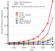
Solar cells are manufactured in volume in Japan, Germany, China, Taiwan, Malaysia and the United States, whereas Europe, China, the U.S., and Japan have dominated (94% or more as of 2013) in installed systems.[120] Other nations are acquiring significant solar cell production capacity.
Global PV cell/module production increased by 10% in 2012 despite a 9% decline in solar energy investments according to the annual "PV Status Report" released by the European Commission's Joint Research Centre. Between 2009 and 2013 cell production has quadrupled.[120][121][122]
China
Due to heavy government investment, China has become the dominant force in solar cell manufacturing. Chinese companies produced solar cells/modules with a capacity of ~23 GW in 2013 (60% of global production).[120]
Malaysia
In 2014, Malaysia was the world's third largest manufacturer of photovoltaics equipment, behind China and the European Union.[123]
United States
Solar cell production in the U.S. has suffered due to the global financial crisis, but recovered partly due to the falling price of quality silicon.[124][125]
See also
- Anomalous photovoltaic effect
- Autonomous building
- Black silicon
- Energy development
- Electromotive force (Solar cell)
- Flexible substrate
- Green technology
- Inkjet solar cell
- List of photovoltaics companies
- List of types of solar cells
- Maximum power point tracking
- Metallurgical grade silicon
- Microgeneration
- Nanoflake
- Photovoltaics
- P–n junction
- Plasmonic solar cell
- Printed electronics
- Quantum efficiency
- Renewable energy
- Roll-to-roll processing
- Shockley-Queisser limit
- Solar Energy Materials and Solar Cells (journal)
- Solar module quality assurance
- Solar roof
- Solar shingles
- Solar tracker
- Solar panel
- Spectrophotometry
- Theory of solar cells
- Thermophotovoltaics
References
- 1 2 Solar Cells. chemistryexplained.com
- ↑ "Solar cells -- performance and use". solarbotics.net.
- ↑ "Technology Roadmap: Solar Photovoltaic Energy" (PDF). IEA. 2014. Archived (PDF) from the original on 7 October 2014. Retrieved 7 October 2014.
- ↑ "Photovoltaic System Pricing Trends – Historical, Recent, and Near-Term Projections, 2014 Edition" (PDF). NREL. 22 September 2014. p. 4. Archived (PDF) from the original on 29 March 2015.
- ↑ Gevorkian, Peter (2007). Sustainable energy systems engineering: the complete green building design resource. McGraw Hill Professional. ISBN 978-0-07-147359-0.
- ↑ "The Nobel Prize in Physics 1921: Albert Einstein", Nobel Prize official page
- ↑ Lashkaryov, V. E. (1941) Investigation of a barrier layer by the thermoprobe method Archived 28 September 2015 at the Wayback Machine., Izv. Akad. Nauk SSSR, Ser. Fiz. 5, 442–446, English translation: Ukr. J. Phys. 53, 53–56 (2008)
- ↑ "Light sensitive device" U.S. Patent 2,402,662 Issue date: June 1946
- ↑ "April 25, 1954: Bell Labs Demonstrates the First Practical Silicon Solar Cell". APS News. American Physical Society. 18 (4). April 2009.
- ↑ Tsokos, K. A. (28 January 2010). Physics for the IB Diploma Full Colour. Cambridge University Press. ISBN 978-0-521-13821-5.
- ↑ Perlin 1999, p. 50.
- 1 2 Perlin 1999, p. 53.
- 1 2 Williams, Neville (2005). Chasing the Sun: Solar Adventures Around the World. New Society Publishers. p. 84. ISBN 9781550923124.
- ↑ Jones, Geoffrey; Bouamane, Loubna (2012). "Power from Sunshine": A Business History of Solar Energy (PDF). Harvard Business School. pp. 22–23.
- ↑ Perlin 1999, p. 54.
- ↑ The National Science Foundation: A Brief History, Chapter IV, NSF 88-16, 15 July 1994 (retrieved 20 June 2015)
- ↑ Herwig, Lloyd O. (1999). "Cherry Hill revisited: Background events and photovoltaic technology status". AIP Conference Proceedings. National center for photovoltaics (NCPV) 15th program review meeting. AIP Conference Proceedings. 462. p. 785. Bibcode:1999AIPC..462..785H. doi:10.1063/1.58015.
- ↑ Deyo, J. N., Brandhorst, H. W., Jr., and Forestieri, A. F., Status of the ERDA/NASA photovoltaic tests and applications project, 12th IEEE Photovoltaic Specialists Conf., 15–18 Nov. 1976
- ↑ Reed Business Information (18 October 1979). The multinational connections-who does what where. Reed Business Information. ISSN 0262-4079.
- ↑ Buhayar, Noah (28 January 2016) Warren Buffett controls Nevada’s legacy utility. Elon Musk is behind the solar company that’s upending the market. Let the fun begin. Bloomberg Businessweek
- ↑ "Sunny Uplands: Alternative energy will no longer be alternative". The Economist. 21 November 2012. Retrieved 28 December 2012.
- ↑ $1/W Photovoltaic Systems DOE whitepaper August 2010
- 1 2 Solar Stocks: Does the Punishment Fit the Crime?. 24/7 Wall St. (6 October 2011). Retrieved 3 January 2012.
- ↑ Parkinson, Giles. "Plunging Cost Of Solar PV (Graphs)". Clean Technica. Retrieved 18 May 2013.
- ↑ "Snapshot of Global PV 1992–2014" (PDF). International Energy Agency — Photovoltaic Power Systems Programme. 30 March 2015. Archived from the original on 30 March 2015.
- ↑ "Solar energy - Renewable energy - Statistical Review of World Energy - Energy economics - BP". bp.com.
- 1 2 Yu, Peng; Wu, Jiang; Liu, Shenting; Xiong, Jie; Jagadish, Chennupati; Wang, Zhiming M. (2016-12-01). "Design and fabrication of silicon nanowires towards efficient solar cells". Nano Today. 11 (6): 704–737. doi:10.1016/j.nantod.2016.10.001.
- ↑ Mann, Sander A.; de Wild-Scholten, Mariska J.; Fthenakis, Vasilis M.; van Sark, Wilfried G.J.H.M.; Sinke, Wim C. (2014-11-01). "The energy payback time of advanced crystalline silicon PV modules in 2020: a prospective study". Progress in Photovoltaics: Research and Applications. 22 (11): 1180–1194. doi:10.1002/pip.2363. ISSN 1099-159X.
- ↑ "BP Global – Reports and publications – Going for grid parity". Archived from the original on 8 June 2011. Retrieved 4 August 2012. . Bp.com. Retrieved 19 January 2011.
- ↑ BP Global – Reports and publications – Gaining on the grid. Bp.com. August 2007.
- ↑ The Path to Grid Parity. bp.com
- ↑ Peacock, Matt (20 June 2012) Solar industry celebrates grid parity, ABC News.
- ↑ Baldwin, Sam (20 April 2011) Energy Efficiency & Renewable Energy: Challenges and Opportunities. Clean Energy SuperCluster Expo Colorado State University. U.S. Department of Energy.
- ↑ ENF Ltd. (8 January 2013). "Small Chinese Solar Manufacturers Decimated in 2012 | Solar PV Business News | ENF Company Directory". Enfsolar.com. Retrieved 1 June 2013.
- ↑ "What is a solar panel and how does it work?". Energuide.be. Sibelga. Retrieved 3 January 2017.
- ↑ Martin, Chris (30 December 2016). "Solar Panels Now So Cheap Manufacturers Probably Selling at Loss". Bloomberg View. Bloomberg LP. Retrieved 3 January 2017.
- ↑ Shankleman, Jessica; Martin, Chris (3 January 2017). "Solar Could Beat Coal to Become the Cheapest Power on Earth". Bloomberg View. Bloomberg LP. Retrieved 3 January 2017.
- 1 2 Kumar, Ankush (2017-01-03). "Predicting efficiency of solar cells based on transparent conducting electrodes". Journal of Applied Physics. 121 (1): 014502. Bibcode:2017JAP...121a4502K. doi:10.1063/1.4973117. ISSN 0021-8979.
- ↑ "Solar Cell Efficiency | PVEducation". www.pveducation.org. Retrieved 2018-01-31.
- ↑ "T.Bazouni: What is the Fill Factor of a Solar Panel". Archived from the original on 15 April 2009. Retrieved 17 February 2009.
- ↑ Rühle, Sven (2016-02-08). "Tabulated Values of the Shockley-Queisser Limit for Single Junction Solar Cells". Solar Energy. 130: 139–147. Bibcode:2016SoEn..130..139R. doi:10.1016/j.solener.2016.02.015.
- ↑ Vos, A. D. (1980). "Detailed balance limit of the efficiency of tandem solar cells". Journal of Physics D: Applied Physics. 13 (5): 839. Bibcode:1980JPhD...13..839D. doi:10.1088/0022-3727/13/5/018.
- ↑ Bullis, Kevin (13 June 2014) Record-Breaking Solar Cell Points the Way to Cheaper Power. MIT Technology Review
- ↑ Dimroth, Frank; Tibbits, Thomas N.D.; Niemeyer, Markus; Predan, Felix; Beutel, Paul; Karcher, Christian; Oliva, Eduard; Siefer, Gerald; Lackner, David; et al. (2016). "Four-Junction Wafer Bonded Concentrator Solar Cells". IEEE Journal of Photovoltaics. 6 (1): 343–349. doi:10.1109/jphotov.2015.2501729.
- 1 2 Janz, Stefan; Reber, Stefan (14 September 2015). "20% Efficient Solar Cell on EpiWafer". Fraunhofer ISE. Retrieved 15 October 2015.
- 1 2 Drießen, Marion; Amiri, Diana; Milenkovic, Nena; Steinhauser, Bernd; Lindekugel, Stefan; Benick, Jan; Reber, Stefan; Janz, Stefan (2016). "Solar Cells with 20% Efficiency and Lifetime Evaluation of Epitaxial Wafers". Energy Procedia. 92: 785–790. doi:10.1016/j.egypro.2016.07.069. ISSN 1876-6102.
- ↑ Zyg, Lisa (4 June 2015). "Solar cell sets world record with a stabilized efficiency of 13.6%". Phys.org.
- ↑ 30.2 Percent Efficiency – New Record for Silicon-based Multi-junction Solar Cell — Fraunhofer ISE. Ise.fraunhofer.de (2016-11-09). Retrieved 2016-11-15.
- ↑ Essig, Stephanie; Allebé, Christophe; Remo, Timothy; Geisz, John F.; Steiner, Myles A.; Horowitz, Kelsey; Barraud, Loris; Ward, J. Scott; Schnabel, Manuel (September 2017). "Raising the one-sun conversion efficiency of III–V/Si solar cells to 32.8% for two junctions and 35.9% for three junctions". Nature Energy. 2 (9). Bibcode:2017NatEn...217144E. doi:10.1038/nenergy.2017.144. ISSN 2058-7546.
- ↑ Gaucher, Alexandre; Cattoni, Andrea; Dupuis, Christophe; Chen, Wanghua; Cariou, Romain; Foldyna, Martin; Lalouat, Loı̈c; Drouard, Emmanuel; Seassal, Christian; Roca i Cabarrocas, Pere; Collin, Stéphane (2016). "Ultrathin Epitaxial Silicon Solar Cells with Inverted Nanopyramid Arrays for Efficient Light Trapping". Nano Letters. 16 (9): 5358. Bibcode:2016NanoL..16.5358G. doi:10.1021/acs.nanolett.6b01240. PMID 27525513.
- ↑ Chen, Wanghua; Cariou, Romain; Foldyna, Martin; Depauw, Valerie; Trompoukis, Christos; Drouard, Emmanuel; Lalouat, Loic; Harouri, Abdelmounaim; Liu, Jia; Fave, Alain; Orobtchouk, Régis; Mandorlo, Fabien; Seassal, Christian; Massiot, Inès; Dmitriev, Alexandre; Lee, Ki-Dong; Cabarrocas, Pere Roca i (2016). "Nanophotonics-based low-temperature PECVD epitaxial crystalline silicon solar cells". Journal of Physics D: Applied Physics. 49 (12): 125603. Bibcode:2016JPhD...49l5603C. doi:10.1088/0022-3727/49/12/125603. ISSN 0022-3727.
- ↑ Kobayashi, Eiji; Watabe, Yoshimi; Hao, Ruiying; Ravi, T. S. (2015). "High efficiency heterojunction solar cells on n-type kerfless mono crystalline silicon wafers by epitaxial growth". Applied Physics Letters. 106 (22): 223504. Bibcode:2015ApPhL.106v3504K. doi:10.1063/1.4922196. ISSN 0003-6951.
- ↑ Kim, D.S.; et al. (18 May 2003). "String ribbon silicon solar cells with 17.8% efficiency" (PDF). Proceedings of 3rd World Conference on Photovoltaic Energy Conversion, 2003. 2: 1293–1296. ISBN 4-9901816-0-3.
- ↑ Wayne McMillan, "The Cast Mono Dilemma" Archived 5 November 2013 at the Wayback Machine., BT Imaging
- ↑ Pearce, J.; Lau, A. (2002). "Net Energy Analysis for Sustainable Energy Production from Silicon Based Solar Cells". Solar Energy (PDF). p. 181. doi:10.1115/SED2002-1051. ISBN 0-7918-1689-3. Archived from the original (PDF) on 2010-06-22.
- ↑ Edoff, Marika (March 2012). "Thin Film Solar Cells: Research in an Industrial Perspective". AMBIO. 41 (2): 112–118. doi:10.1007/s13280-012-0265-6. ISSN 0044-7447. PMC 3357764. PMID 22434436.
- 1 2 Fthenakis, Vasilis M. (2004). "Life cycle impact analysis of cadmium in CdTe PV production" (PDF). Renewable and Sustainable Energy Reviews. 8 (4): 303–334. doi:10.1016/j.rser.2003.12.001.
- ↑ "IBM and Tokyo Ohka Kogyo Turn Up Watts on Solar Energy Production", IBM
- ↑ Collins, R. W.; Ferlauto, A. S.; Ferreira, G. M.; Chen, C.; Koh, J.; Koval, R. J.; Lee, Y.; Pearce, J. M.; Wronski, C. R. (2003). "Evolution of microstructure and phase in amorphous, protocrystalline, and microcrystalline silicon studied by real time spectroscopic ellipsometry". Solar Energy Materials and Solar Cells. 78: 143. doi:10.1016/S0927-0248(02)00436-1.
- ↑ Pearce, J. M.; Podraza, N.; Collins, R. W.; Al-Jassim, M. M.; Jones, K. M.; Deng, J.; Wronski, C. R. (2007). "Optimization of open circuit voltage in amorphous silicon solar cells with mixed-phase (amorphous+nanocrystalline) p-type contacts of low nanocrystalline content" (PDF). Journal of Applied Physics. 101 (11): 114301. Bibcode:2007JAP...101k4301P. doi:10.1063/1.2714507. Archived from the original (PDF) on 13 June 2009.
- ↑ Yablonovitch, Eli; Miller, Owen D.; Kurtz, S. R. (2012). "The opto-electronic physics that broke the efficiency limit in solar cells". 2012 38th IEEE Photovoltaic Specialists Conference. p. 001556. doi:10.1109/PVSC.2012.6317891. ISBN 978-1-4673-0066-7.
- ↑ "Photovoltaics Report" (PDF). Fraunhofer ISE. 28 July 2014. Archived (PDF) from the original on 31 August 2014. Retrieved 31 August 2014.
- ↑ Oku, Takeo; Kumada, Kazuma; Suzuki, Atsushi; Kikuchi, Kenji (June 2012). "Effects of germanium addition to copper phthalocyanine/fullerene-based solar cells". Central European Journal of Engineering. 2 (2): 248–252. Bibcode:2012CEJE....2..248O. doi:10.2478/s13531-011-0069-7.
- ↑ Triple-Junction Terrestrial Concentrator Solar Cells. (PDF) Retrieved 3 January 2012.
- ↑ Clarke, Chris (19 April 2011) San Jose Solar Company Breaks Efficiency Record for PV. Optics.org. Retrieved 19 January 2011.
- ↑ Cariou, Romain; Chen, Wanghua; Maurice, Jean-Luc; Yu, Jingwen; Patriarche, Gilles; Mauguin, Olivia; Largeau, Ludovic; Decobert, Jean; Roca i Cabarrocas, Pere (2016). "Low temperature plasma enhanced CVD epitaxial growth of silicon on GaAs: a new paradigm for III-V/Si integration". Scientific Reports. 6: 25674. Bibcode:2016NatSR...625674C. doi:10.1038/srep25674. ISSN 2045-2322. PMC 4863370. PMID 27166163.
- ↑ "NREL effiiciency chart". Archived from the original on 22 January 2016.
- ↑ Kosasih, Felix Utama; Ducati, Caterina (May 2018). "Characterising degradation of perovskite solar cells through in-situ and operando electron microscopy". Nano Energy. 47: 243–256. doi:10.1016/j.nanoen.2018.02.055.
- ↑ "Radiation energy transducing device". Mori Hiroshi, Hayakawa Denki Kogyo KK. 1961-10-03.
- ↑ (A1) ES 453575 (A1) A. Luque: "Procedimiento para obtener células solares bifaciales" filing date 05.05.1977
- ↑ (A) US 4169738 (A) A. Luque: "Double-sided solar cell with self-refrigerating concentrator" filing date 21.11.1977
- ↑ Luque, A.; Cuevas, A.; Eguren, J. (1978). "Solar-Cell Behavior under Variable Surface Recombination Velocity and Proposal of a Novel Structure". Solid-State Electronics. 21 (5): 793–794. Bibcode:1978SSEle..21..793L. doi:10.1016/0038-1101(78)90014-X.
- ↑ Cuevas, A.; Luque, A.; Eguren, J.; Alamo, J. del (1982). "50 Per cent more output power from an albedo-collecting flat panel using bifacial solar cells". Solar Energy. 29 (5): 419–420. Bibcode:1982SoEn...29..419C. doi:10.1016/0038-092x(82)90078-0.
- ↑ "International Technology Roadmap for Photovoltaic (ITRPV) - Home". www.itrpv.net. Retrieved 2018-02-20.
- 1 2 Sun, Xingshu; Khan, Mohammad Ryyan; Deline, Chris; Alam, Muhammad Ashraful. "Optimization and performance of bifacial solar modules: A global perspective". Applied Energy. 212: 1601–1610. doi:10.1016/j.apenergy.2017.12.041.
- ↑ Khan, M. Ryyan; Hanna, Amir; Sun, Xingshu; Alam, Muhammad A. "Vertical bifacial solar farms: Physics, design, and global optimization". Applied Energy. 206: 240–248. doi:10.1016/j.apenergy.2017.08.042.
- ↑ Zhao, Binglin; Sun, Xingshu; Khan, Mohammad Ryyan; Alam, Muhammad Ashraful (2018-02-19). "Purdue Bifacial Module Calculator". doi:10.4231/d3542jb3c.
- ↑ Luque, Antonio, and Antonio Martí. "Increasing the Efficiency of Ideal Solar Cells by Photon Induced Transitions at Intermediate Levels." Physical Review Letters 78.26 (1997): 5014-017. Web.
- ↑ Okada, Yoshitaka, Tomah Sogabe, and Yasushi Shoji. "Chapter 13: "Intermediate Band Solar Cells"" Advanced Concepts in Photovoltaics. Ed. Arthur J. Nozik, Gavin Conibeer, and Matthew C. Beard. Vol. No. 11. Cambridge, UK: Royal Society of Chemistry, 2014. 425-54. Print. RSC Energy and Environment Ser.
- ↑ Researchers use liquid inks to create better solar cells, Phys.org, 17 September 2014, Shaun Mason
- ↑ Hernández-Rodríguez, M.A.; Imanieh, M.H.; Martín, L.L.; Martín, I.R. (September 2013). "Experimental enhancement of the photocurrent in a solar cell using upconversion process in fluoroindate glasses exciting at 1480nm". Solar Energy Materials and Solar Cells. 116: 171–175. doi:10.1016/j.solmat.2013.04.023.
- ↑ Dye Sensitized Solar Cells. G24i.com (2 April 2014). Retrieved 20 April 2014.
- ↑ "Quantum dot sensitized solar cell: Recent advances and future perspectives in photoanode". Solar Energy Materials and Solar Cells. 155: 294–322. 2016-10-01. doi:10.1016/j.solmat.2016.05.062. ISSN 0927-0248.
- ↑ Semonin, O. E.; Luther, J. M.; Choi, S.; Chen, H.-Y.; Gao, J.; Nozik, A. J.; Beard, M. C. (2011). "Peak External Photocurrent Quantum Efficiency Exceeding 100% via MEG in a Quantum Dot Solar Cell". Science. 334 (6062): 1530–3. Bibcode:2011Sci...334.1530S. doi:10.1126/science.1209845. PMID 22174246.
- ↑ Kamat, Prashant V. (2012). "Boosting the Efficiency of Quantum Dot Sensitized Solar Cells through Modulation of Interfacial Charge Transfer". Accounts of Chemical Research. 45 (11): 120411095315008. doi:10.1021/ar200315d.
- ↑ Santra, Pralay K.; Kamat, Prashant V. (2012). "Mn-Doped Quantum Dot Sensitized Solar Cells: A Strategy to Boost Efficiency over 5%". Journal of the American Chemical Society. 134 (5): 2508–11. doi:10.1021/ja211224s. PMID 22280479.
- ↑ Moon, Soo-Jin; Itzhaik, Yafit; Yum, Jun-Ho; Zakeeruddin, Shaik M.; Hodes, Gary; GräTzel, Michael (2010). "Sb2S3-Based Mesoscopic Solar Cell using an Organic Hole Conductor". The Journal of Physical Chemistry Letters. 1 (10): 1524. doi:10.1021/jz100308q.
- ↑ Zn–Cu–In–Se Quantum Dot Solar Cells with a Certified Power Conversion Efficiency of 11.6% Jun Du, Zhonglin Du, Jin-Song Hu, Zhenxiao Pan, Qing Shen, Jiankun Sun, Donghui Long, Hui Dong, Litao Sun, Xinhua Zhong, and Li-Jun Wan 2016 138 (12), 4201-4209 DOI: 10.1021/jacs.6b00615
- ↑ Solar Cell Research || The Prashant Kamat lab at the University of Notre Dame. Nd.edu (22 February 2007). Retrieved 17 May 2012.
- ↑ Genovese, Matthew P.; Lightcap, Ian V.; Kamat, Prashant V. (2012). "Sun-BelievableSolar Paint. A Transformative One-Step Approach for Designing Nanocrystalline Solar Cells". ACS Nano. 6 (1): 865–72. doi:10.1021/nn204381g. PMID 22147684.
- 1 2 Yu, Peng; Wu, Jiang; Gao, Lei; Liu, Huiyun; Wang, Zhiming (2017-03-01). "InGaAs and GaAs quantum dot solar cells grown by droplet epitaxy". Solar Energy Materials and Solar Cells. 161: 377–381. doi:10.1016/j.solmat.2016.12.024.
- ↑ Wu, Jiang; Yu, Peng; Susha, Andrei S.; Sablon, Kimberly A.; Chen, Haiyuan; Zhou, Zhihua; Li, Handong; Ji, Haining; Niu, Xiaobin (2015-04-01). "Broadband efficiency enhancement in quantum dot solar cells coupled with multispiked plasmonic nanostars". Nano Energy. 13: 827–835. doi:10.1016/j.nanoen.2015.02.012.
- ↑ Konarka Power Plastic reaches 8.3% efficiency. pv-tech.org. Retrieved 7 May 2011.
- ↑ Mayer, A.; Scully, S.; Hardin, B.; Rowell, M.; McGehee, M. (2007). "Polymer-based solar cells". Materials Today. 10 (11): 28. doi:10.1016/S1369-7021(07)70276-6.
- ↑ Lunt, R. R.; Bulovic, V. (2011). "Transparent, near-infrared organic photovoltaic solar cells for window and energy-scavenging applications". Applied Physics Letters. 98 (11): 113305. Bibcode:2011ApPhL..98k3305L. doi:10.1063/1.3567516.
- ↑ Rudolf, John Collins (20 April 2011). "Transparent Photovoltaic Cells Turn Windows Into Solar Panels". green.blogs.nytimes.com.
- ↑ "UCLA Scientists Develop Transparent Solar Cell". Enviro-News.com. 24 July 2012. Archived from the original on 27 July 2012.
- ↑ Lunt, R. R.; Osedach, T. P.; Brown, P. R.; Rowehl, J. A.; Bulović, V. (2011). "Practical Roadmap and Limits to Nanostructured Photovoltaics". Advanced Materials. 23 (48): 5712–27. doi:10.1002/adma.201103404. PMID 22057647.
- ↑ Lunt, R. R. (2012). "Theoretical limits for visibly transparent photovoltaics". Applied Physics Letters. 101 (4): 043902. Bibcode:2012ApPhL.101d3902L. doi:10.1063/1.4738896.
- ↑ Guo, C.; Lin, Y. H.; Witman, M. D.; Smith, K. A.; Wang, C.; Hexemer, A.; Strzalka, J.; Gomez, E. D.; Verduzco, R. (2013). "Conjugated Block Copolymer Photovoltaics with near 3% Efficiency through Microphase Separation". Nano Letters. 13 (6): 2957–63. Bibcode:2013NanoL..13.2957G. doi:10.1021/nl401420s. PMID 23687903.
- ↑ "Organic polymers create new class of solar energy devices". Kurzweil Accelerating Institute. 31 May 2013. Retrieved 1 June 2013.
- 1 2 Bullis, Kevin (30 July 2014) Adaptive Material Could Cut the Cost of Solar in Half. MIT Technology Review
- ↑ Campbell, Patrick; Green, Martin A. (Feb 1987). "Light Trapping Properties of Pyramidally textured surfaces". Journal of Applied Physics. 62: 243–249. Bibcode:1987JAP....62..243C. doi:10.1063/1.339189.
- ↑ Zhao, Jianhua; Wang, Aihua; Green, Martin A. (May 1998). "19.8% efficient "honeycomb" textured multicrystalline and 24.4% monocrystalline silicon solar cells". Applied Physics Letters. 73 (14): 1991–1993. Bibcode:1998ApPhL..73.1991Z. doi:10.1063/1.122345.
- ↑ Hauser, H.; Michl, B.; Kubler, V.; Schwarzkopf, S.; Muller, C.; Hermle, M.; Blasi, B. (2011). "Nanoimprint Lithography for Honeycomb Texturing of Multicrystalline Silicon". Energy Procedia. 8: 648–653. doi:10.1016/j.egypro.2011.06.196.
- ↑ Tucher, Nico; Eisenlohr, Johannes; Gebrewold, Habtamu; Kiefel, Peter; Höhn, Oliver; Hauser, Hubert; Goldschmidt, Jan Christoph; Bläsi, Benedikt (2016-07-11). "Optical simulation of photovoltaic modules with multiple textured interfaces using the matrix-based formalism OPTOS". Optics Express. 24 (14): A1083–A1093. Bibcode:2016OExpr..24A1083T. doi:10.1364/OE.24.0A1083.
- ↑ Mavrokefalos, Anastassios; Han, Sang Eon.; Yerci, Selcuk; Branham, M.S.; Chen, Gang. (June 2012). "Efficient Light Trapping in Inverted Nanopyramid Thin Crystalline Silicon Membranes for Solar Cell Applications". Nano Letters. 12 (6): 2792–2796. Bibcode:2012NanoL..12.2792M. doi:10.1021/nl2045777. PMID 22612694.
- ↑ Jaus, J.; Pantsar, H.; Eckert, J.; Duell, M.; Herfurth, H.; Doble, D. (2010). "Light management for reduction of bus bar and gridline shadowing in photovoltaic modules". 2010 35th IEEE Photovoltaic Specialists Conference. p. 000979. doi:10.1109/PVSC.2010.5614568. ISBN 978-1-4244-5890-5.
- ↑ Mingareev, I.; Berlich, R.; Eichelkraut, T. J.; Herfurth, H.; Heinemann, S.; Richardson, M. C. (2011-06-06). "Diffractive optical elements utilized for efficiency enhancement of photovoltaic modules". Optics Express. 19 (12): 11397. Bibcode:2011OExpr..1911397M. doi:10.1364/OE.19.011397.
- ↑ Uematsu, T; Yazawa, Y; Miyamura, Y; Muramatsu, S; Ohtsuka, H; Tsutsui, K; Warabisako, T (2001-03-01). "Static concentrator photovoltaic module with prism array". Solar Energy Materials and Solar Cells. PVSEC 11 - PART III. 67 (1–4): 415–423. doi:10.1016/S0927-0248(00)00310-X.
- 1 2 Chen, Fu-hao; Pathreeker, Shreyas; Kaur, Jaspreet; Hosein, Ian D. (2016-10-31). "Increasing light capture in silicon solar cells with encapsulants incorporating air prisms to reduce metallic contact losses". Optics Express. 24 (22): A1419. Bibcode:2016OExpr..24A1419C. doi:10.1364/oe.24.0a1419.
- ↑ Korech, Omer; Gordon, Jeffrey M.; Katz, Eugene A.; Feuermann, Daniel; Eisenberg, Naftali (2007-10-01). "Dielectric microconcentrators for efficiency enhancement in concentrator solar cells". Optics Letters. 32 (19): 2789. Bibcode:2007OptL...32.2789K. doi:10.1364/OL.32.002789.
- ↑ Hosein, Ian D.; Lin, Hao; Ponte, Matthew R.; Basker, Dinesh K.; Saravanamuttu, Kalaichelvi (2013-11-03). "Enhancing Solar Energy Light Capture with Multi-Directional Waveguide Lattices". Renewable Energy and the Environment: RM2D.2. doi:10.1364/OSE.2013.RM2D.2. ISBN 978-1-55752-986-2.
- ↑ Biria, Saeid; Chen, Fu Hao; Pathreeker, Shreyas; Hosein, Ian D. (2017-12-22). "Polymer Encapsulants Incorporating Light-Guiding Architectures to Increase Optical Energy Conversion in Solar Cells". Advanced Materials. 30 (8): 1705382. doi:10.1002/adma.201705382. ISSN 0935-9648.
- ↑ Huang, Zhiyuan; Li, Xin; Mahboub, Melika; Hanson, Kerry M.; Nichols, Valerie M.; Le, Hoang; Tang, Ming L.; Bardeen, Christopher J. (2015-08-12). "Hybrid Molecule–Nanocrystal Photon Upconversion Across the Visible and Near-Infrared". Nano Letters. 15 (8): 5552–5557. Bibcode:2015NanoL..15.5552H. doi:10.1021/acs.nanolett.5b02130. PMID 26161875.
- ↑ Schumann, Martin F.; Langenhorst, Malte; Smeets, Michael; Ding, Kaining; Paetzold, Ulrich W.; Wegener, Martin (2017-07-04). "All-Angle Invisibility Cloaking of Contact Fingers on Solar Cells by Refractive Free-Form Surfaces". Advanced Optical Materials. 5 (17): 1700164. doi:10.1002/adom.201700164. ISSN 2195-1071.
- ↑ "Freeform surface invisibility cloaking of interconnection lines in thin-film photovoltaic modules". Solar Energy Materials and Solar Cells. 182: 294–301. 2018-08-01. doi:10.1016/j.solmat.2018.03.034. ISSN 0927-0248.
- ↑ Fitzky, Hans G. and Ebneth, Harold (24 May 1983) U.S. Patent 4,385,102, "Large-area photovoltaic cell"
- ↑ Pv News November 2012. Greentech Media. Retrieved 3 June 2012.
- 1 2 3 Jäger-Waldau, Arnulf (September 2013) PV Status Report 2013. European Commission, Joint Research Centre, Institute for Energy and Transport.
- ↑ PV production grows despite a crisis-driven decline in investment. European Commission, Brussels, 30 September 2013
- ↑ PV Status Report 2013 | Renewable Energy Mapping and Monitoring in Europe and Africa (REMEA). Iet.jrc.ec.europa.eu (11 April 2014). Retrieved 20 April 2014.
- ↑ "Solar Rises in Malaysia During Trade Wars Over Panels". New York Times. 12 December 2014.
- ↑ Plunging Cost Of Solar PV (Graphs). CleanTechnica (7 March 2013). Retrieved 20 April 2014.
- ↑ Falling silicon prices shakes up solar manufacturing industry. Down To Earth (19 September 2011). Retrieved 20 April 2014.
Bibliography
- Perlin, John (1999). From space to Earth: the story of solar electricity. Earthscan. p. 50. ISBN 978-0-937948-14-9.
External links
| Wikimedia Commons has media related to Photovoltaics. |
| Wikimedia Commons has media related to solar cell. |
- PV Lighthouse Calculators and Resources for photovoltaic scientists and engineers
- Photovoltaics CDROM online
- Solar cell manufacturing techniques
- Renewable Energy: Solar at Curlie (based on DMOZ)
- Solar Energy Laboratory at University of Southampton
- NASA's Photovoltaic Info
- Green, M. A.; Emery, K.; Hishikawa, Y.; Warta, W. (2010). "Solar cell efficiency tables (version 36)". Progress in Photovoltaics: Research and Applications. 18 (5): 346. doi:10.1002/pip.1021.
- "Electric Energy From Sun Produced by Light Cell" Popular Mechanics, July 1931 article on various 1930s research on solar cells
- Advantages and disadvantages different solar cells types
- What is solar system for home and how much will the cost of on grid solar and off grid solar system?