Molecular-beam epitaxy
Molecular-beam epitaxy (MBE) is an epitaxy method for thin-film deposition of single crystals. The MBE process was developed in the late 1960s at Bell Telephone Laboratories by J. R. Arthur and Alfred Y. Cho.[1][2] MBE is widely used in the manufacture of semiconductor devices, including transistors, and it is considered one of the fundamental tools for the development of the nanotechnologies.[3]
Method
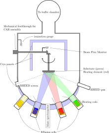
Molecular-beam epitaxy takes place in high vacuum or ultra-high vacuum (10−8–10−12 Torr). The most important aspect of MBE is the deposition rate (typically less than 3,000 nm per hour) that allows the films to grow epitaxially. These deposition rates require proportionally better vacuum to achieve the same impurity levels as other deposition techniques. The absence of carrier gases, as well as the ultra-high vacuum environment, result in the highest achievable purity of the grown films.
In solid source MBE, elements such as gallium and arsenic, in ultra-pure form, are heated in separate quasi-Knudsen effusion cells or electron-beam evaporators until they begin to slowly sublime. The gaseous elements then condense on the wafer, where they may react with each other. In the example of gallium and arsenic, single-crystal gallium arsenide is formed. When evaporation sources such as copper or gold are used, the gaseous elements impinging on the surface may be adsorbed (after a time window where the impinging atoms will hop around the surface) or reflected. Atoms on the surface may also desorb. Controlling the temperature of the source will control the rate of material impinging on the substrate surface and the temperature of the substrate will affect the rate of hopping or desorption. The term "beam" means that evaporated atoms do not interact with each other or vacuum-chamber gases until they reach the wafer, due to the long mean free paths of the atoms.
During operation, reflection high-energy electron diffraction (RHEED) is often used for monitoring the growth of the crystal layers. A computer controls shutters in front of each furnace, allowing precise control of the thickness of each layer, down to a single layer of atoms. Intricate structures of layers of different materials may be fabricated this way. Such control has allowed the development of structures where the electrons can be confined in space, giving quantum wells or even quantum dots. Such layers are now a critical part of many modern semiconductor devices, including semiconductor lasers and light-emitting diodes.
In systems where the substrate needs to be cooled, the ultra-high vacuum environment within the growth chamber is maintained by a system of cryopumps and cryopanels, chilled using liquid nitrogen or cold nitrogen gas to a temperature close to 77 kelvins (−196 degree Celsius). Cold surfaces act as a sink for impurities in the vacuum, so vacuum levels need to be several orders of magnitude better to deposit films under these conditions. In other systems, the wafers on which the crystals are grown may be mounted on a rotating platter, which can be heated to several hundred degrees Celsius during operation.
Molecular-beam epitaxy is also used for the deposition of some types of organic semiconductors. In this case, molecules, rather than atoms, are evaporated and deposited onto the wafer. Other variations include gas-source MBE, which resembles chemical vapor deposition.
MBE systems can also be modified accordingly to the needs. Oxygen sources, for examples, can be incorporated for depositing oxide materials for advanced electronic, magnetic and optical applications, as well as for fundamental research.
Quantum nanostructures
One of the most accomplished achievements of MBE is the nano-structures that permitted the formation of atomically flat and abrupt hetero-interfaces. Such structures have played an unprecedented role in expanding the knowledge of physics and electronics[4]. Most recently the construction of nanowires and quantum structures built within them that allow information processing and the possible integration with on-chip applications for quantum communication and computing[5]. These heterostructure nanowire lasers are only possible to build using advance MBE techniques, allowing monolithical integration on silicon[6] and picosecond signal processing[7].
Asaro–Tiller–Grinfeld instability
The Asaro–Tiller–Grinfeld (ATG) instability, also known as the Grinfeld instability, is an elastic instability often encountered during molecular-beam epitaxy. If there is a mismatch between the lattice sizes of the growing film and the supporting crystal, elastic energy will be accumulated in the growing film. At some critical height, the free energy of the film can be lowered if the film breaks into isolated islands, where the tension can be relaxed laterally. The critical height depends on the Young's modulus, mismatch size, and surface tension.
Some applications for this instability have been researched, such as the self-assembly of quantum dots. This community uses the name of Stranski–Krastanov growth for ATG.
See also
Notes
- ↑ Cho, A. Y.; Arthur, J. R.; Jr (1975). "Molecular beam epitaxy". Prog. Solid State Chem. 10: 157–192. doi:10.1016/0079-6786(75)90005-9.
- ↑ Gwo-Ching Wang, Toh-Ming Lu (2013). RHEED Transmission Mode and Pole Figures. doi:10.1007/978-1-4614-9287-0.
- ↑ McCray, W.P. (2007). "MBE Deserves a Place in the History Books". Nature Nanotechnology. 2 (5): 259–261. Bibcode:2007NatNa...2..259M. doi:10.1038/nnano.2007.121.
- ↑ http://ieeexplore.ieee.org/document/1037732/?reload=true
- ↑ http://pubs.rsc.org/en/content/articlelanding/2013/tc/c3tc30556b
- ↑ Mayer, B., et al. "Monolithically integrated high-β nanowire lasers on silicon". Nano letters 16.1 (2015): 152–156.
- ↑ Mayer, B., et al. "Long-term mutual phase locking of picosecond pulse pairs generated by a semiconductor nanowire laser". Nature Communications 8 (2017): 15521.
References
- Jaeger, Richard C. (2002). "Film Deposition". Introduction to Microelectronic Fabrication (2nd ed.). Upper Saddle River: Prentice Hall. ISBN 0-201-44494-1.
- McCray, W. P. (2007). "MBE Deserves a Place in the History Books". Nature Nanotechnology. 2 (5): 259–261. Bibcode:2007NatNa...2..259M. doi:10.1038/nnano.2007.121.
- Shchukin, Vitaliy A.; Dieter Bimberg (1999). "Spontaneous ordering of nanostructures on crystal surfaces". Reviews of Modern Physics. 71 (4): 1125–1171. Bibcode:1999RvMP...71.1125S. doi:10.1103/RevModPhys.71.1125.
- Stangl, J.; V. Holý; G. Bauer (2004). "Structural properties of self-organized semiconductor nanostructures". Reviews of Modern Physics. 76 (3): 725–783. Bibcode:2004RvMP...76..725S. doi:10.1103/RevModPhys.76.725.
Further reading
- Frigeri, P.; Seravalli, L.; Trevisi, G.; Franchi, S. (2011). "3.12: Molecular Beam Epitaxy: An Overview". In Pallab Bhattacharya, Roberto Fornari, and Hiroshi Kamimura. Comprehensive Semiconductor Science and Technology. 3. Amsterdam: Elsevier. pp. 480–522. doi:10.1016/B978-0-44-453153-7.00099-7. ISBN 9780444531537.
External links
- Veeco MBE: A manufacturer of MBE systems and effusion cells
- Silicon and germanium nanowires by molecular beam epitaxy
- University of Texas MBE group (Primer on MBE growth)
- Physics of Thin Films: Molecular Beam Epitaxy (class notes)
- CrystalXE.com: a specialized software for molecular-beam epitaxy