Center of Excellence in Nanotechnology
 CoEN @ AIT | |
| Motto | There is no sky to limit us at the bottom |
|---|---|
| Type | Center of Excellence |
| Endowment | NANOTEC, NSTDA |
| Director | Prof. Louis G. Horniyak |
Academic staff | 6 |
Administrative staff | 5 |
| Students | 23 |
| Postgraduates | 23 |
| 11 | |
| Location | Klong Luang, Bangkok, Pathum Thani, Thailand |
| Campus | Suburban |
| Website | http://www.nano.ait.asia |
|
| |
The Center of Excellence (CoE) in Nanotechnology is located inside the Asian Institute of Technology campus. It is one among the eight centers of excellence in Thailand.
The CoEN at AIT is about applied research and graduate education in the field of nanotechnology. The unifying concept in the center's research activities is to make use of inexpensive wet-chemical methods to fabricate innovative materials and futuristic device components. Current research activities at the CoEN focuses on dye-sensitized solar cells, piezotronic devices, gas sensors, bio-diagnostic tools, specific microbial sensors, heavy metal ion sensors for waste water, environmental mitigation through visible light photocatalysis, self-organisation of nanoparticles, and layer-by layer growth from colloidal particles, among others. Master's degree program in Nanotechnology has been launched in 2009. The center has over 30 members from 10 different countries who are carrying out cutting-edge cross-disciplinary research in nanotechnology.
Notable international collaborations are with: State University of New York, Buffalo, USA;[1] S N Bose National Centre for Basic Science,[2] India; Center of Photoelectrochemical Energy, Korea University, Jochiwon, South Korea;[3] Center for Nanobioscience, Agharkar Institute, India;[4] Inorganic Materials Laboratory, Royal Institute of Technology, Stockholm, Sweden; Swiss Federal Institute of Technology, Switzerland;[5] Uppsala University, Sweden;[6] University of Quebec, Canada;[7] Leibniz Institute of New Materials, Germany; University of California, Berkeley, USA;[8] and Griffith University, Australia.[9]
History

The Center of Excellence in Nanotechnology was started in 2006 with an aim to address the creation of knowledge in areas relevant to Thailand, its industries and its people. Activities include joint research with other local and international universities and institutes, education and training personnel in the field of nanotechnology, technology transfer and promotion of public and industrial awareness of nanotechnology. This center provides international platform for academicians and researchers from Thailand, AIT and our partnered universities worldwide to work together in partnership with the industries.
In Thailand, there are currently 8 Centers of Excellence under Thailand National Nanotechnology Center: NANOTEC: CoE Kasetsert University, Bangkok; CoE Chulalongkorn University, Bangkok; CoE King Mongkut Institute of Technology Ladkrabang, Bangkok; CoE Mahidol University, Bangkok; CoE Asian Institute of Technology, Pathum Thani; CoE Prince of Songkhla University, Phuket; CoE Khon Kaen University, Khon Kaen; and CoE Chiang Mai University, Chiang Mai.
The Center of Excellence in Nanotechnology at AIT was set up, jointly with the National Nanotechnology Center, Thailand of the NSTDA,[11] at the Asian Institute of Technology campus, Thailand. Under the agreement, AIT and NANOTEC supports the center jointly. A few faculties at AIT joined hands to propose for this center to be established in the institute. The faculties came from all the three schools and the founding members were: Prof. Joydeep Dutta,[10] Prof. W. Kanok-Nukulchai,[12] Dr. Oleg Shipin,[13] Late Dr. N. Coowanitwong,[14] Dr. M. Parnichkun,[15] Dr. Mousa M. Nazhad,[16] Dr. S. Venkatesh[17] and Dr. P. Herabat.[18] A few rooms in the Chalarm Prakiat Building in Asian Institute of Technology were allocated for its operation. Initially, due to the lack of sufficient funds the center had a hard time to start performing. Prof. Joydeep Dutta,[10] CoEN Director, recalls, "I used to get glasses and mugs from my house to fulfill the students requirements for glasswares in the lab." Over the years the center got crowded with new equipment coming in and more researchers joining the nano-team. Eventually in September 2009, the center was officially shifted to the Outreach building.
On 8 September 2009, a state-of-the-art facility of the Center of Excellence in Nanotechnology at AIT was jointly inaugurated by Prof. Said Irandoust,[19] AIT President, and Dr. Paritud Bhandhubanyong,[20] Director, National Metal and Materials Technology Center.[21] The lab had bigger and larger space and was more free for the visitors from outside.
Administration
The Asian Institute of Technology governs the administrative activities of the Center of Excellence in Nanotechnology. Prof. Joydeep Dutta,[10] is the director of CoEN.
Campus
The facilities provided for the students in AIT is freely available to the researchers and students of the center. With a clean and green campus and sporting facilities such as football grounds, tennis fields, badminton, volleyball, basketball courts, a swimming pool, a golf course etc., the students can find time for recreation and physical workouts within the campus. A two-storied library is accessible to all the members of AIT.
Academics
Doctoral research in Nanotechnology was taking place since 2003. But, Master's degree program in Nanotechnology at AIT was recently launched in August 2009.[22] It has attracted considerable interest amongst students across Asia. The program is open to graduates with Bachelor of engineering (electrical, chemical, mechanical, industrial, telecommunications, computer engineering, electronics, and instrumentation) as well as Bachelor of Science (physics and chemistry).
Essential features of AIT's Nanotechnology degree program are: programmatic balance; processing nanostructures properties applications (P-N-P-A); interdisciplinarity; science (including biology) and technology; integrated classroom-lab experience; hands-on experiments and use of instrumentations; curriculum linked to applications; balance between theory and practice (industrial needs); and content addressing societal impact: public safety, ethics, and awareness.
Courses offered
The aim of the ‘integrated Master’s degree programme in Nanotechnology’ is to address the knowledge-based industries of the 21st century that will require continuous development of their workforce in this new field as well as a technically updated management. The Nanotechnology course is designed in such a way that students from different disciplines can get easily acquainted with the subject matter. Prof. Dutta, Director, CoeN at AIT, and Prof. G. Louis Hornyak,[23] visiting faculty, are teaching students from different backgrounds such as Material sciences, Chemistry, Physics, Agriculture etc. The Nanotechnology master's degree program is designed to be multidisciplinary covering areas such as:
- The macroscopic and microscopic world
- Physics/electronics
- Chemistry/chemical engg.
- Biotechnology
- Material sciences
- Microsystem technology
- Instrumentation
- Environment
The list of the courses offered under School or an Institute-Level course: School of engineering and Technology and Area/Field of Study: Nanotechnology in AIT website[24] is given below:
- Self Assembly and molecular manufacturing (January)
- Impact of Nanotechnology on the Society (August)
- Intellectual Property Rights for Technology Development and Management (August)
- Solid State Physics for Nanotechnology (January)
- Fundamentals of Chemistry (August)
- Catalysis (August)
- Nano Thermodynamics (January)
- Nanomaterials and Nanotechnology (January)
- Colloids and Nanoparticles (August)
- Microelectronics Fabrication Technology (August)
- Microelectromechanical and Nanoelectromechanical systems (January)
- Characterization Tools in Nanotechnology (January)
- Advanced Seminars in Nanotechnology (January)
Research
The Center of Excellence in Nanotechnology has acquired synthesis experience of nanoparticles by reactive precipitation techniques. Gold, silver, platinum, palladium, zinc sulphide, zinc oxide and silica nanoparticles are synthesized regularly at the center for a variety of applications. The platform technology of the center can be discussed as follows:
- Nanoparticles: gold, silver, platinum, palladium, silica, zinc oxide, zinc sulphide
- Nanowires: zinc oxide
- Coating Techniques: sol-gel coating, pyrosol coating, layer by layer organization, Ink-Jet printing, spin coating

The research efforts in AIT center are broadly classified into three groups:
- Environment: photocatalysis, heavy metal ion sensors, bacteria sensing, self-cleaning windows
- Agriculture and Food: E. coli sensors, E. nose, smart pesticides, gas sensors
- Alternate Energy Harvesting: nano-bio solar cells, nano-energy generators
Primary objective of the center is to seek applications of nanoparticles. Research work has extended to nanowires and extensive work is being carried out especially in the environmental application and the energy harvesting side for the application of nanowires on zinc oxide. The competence achieved at the CoEN in AIT has been primarily in the synthesis of metal nanoparticles like gold, silver, platinum and palladium, and zinc compounds namely zinc oxide and zinc sulphide. Some additional work on the development of sol-gel type titanium dioxide has also taken place. Doping of semiconductor nanoparticles and studies on the defect engineering of metal oxides have been another key area of research at the center with an objective to apply the added value obtained from defect engineering into some applications.
Synthesis of Nanoparticles
The different methods employed to synthesize nanoparticles of gold, silver, zinc sulphide, zinc oxide, silica among other is briefly given below:

Gold Nanoparticles
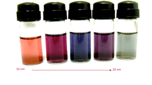
Generally, gold nanoparticles in aqueous solutions are synthesized by the reduction of hydrogen tetrachloroaurate (HAuCl4). To prevent the particles so formed from aggregating, often stabilizing agents are added. During the process, tri-sodium citrate reduces the gold salt to metallic gold particles, which acts as seeds for continuous growth.
Silver Nanoparticles

The silver nanoparticles are synthesized by chemical reduction of silver nitrate. The reducing reagent used for the synthesis of silver nanoparticles are similar to the Turkevitch method, i.e. using tri-sodium citrate. After creation of nanoparticle colloid, in order to increase the viscosity for jetting the inks, polymers such as Chitosan, Poly Vinyl Alcohol (PVA) and Poly Ethylene Glycol (PEG) are added to stabilize the solution.
ZnS Nanoparticles

The organometallic synthesis of ZnS:Mn2+ nanoparticles developed is similar to the method described by Bhargava et al.
ZnO Nanoparticles
ZnO nanoparticles are synthesized in three different solvents and their optical absorptions studied to determine in which solvent the nanoparticles absorb maximum visible light in the optical band ranging between 400 nm and 700 nm. The nanoparticles synthesized in different solvents (isopropanol, methanol and ethanol) by the standard methods as explained in the experimental section yielded nanoparticles which are almost comparable in size (5 to 7 nm).
Silica Nanoparticles
Silica nanoparticles can be synthesized by sol-gel method – Stöber et al. published process for synthesize silica particles by hydrolysis of tetraethyl orthosilicate (TEOS) in ethanol solution – which is catalyzed by ammonia (NH3). Monodispersed silica spheres can be achieved from hydrolysis and condensation of alkoxide silicon by the following methods:
Hydrolysis: to form silanol groups
- Si(OR)
4+ H
2O → Si(OH)
4+ 4(R-OH)
Condensation : to form siloxame bridges
- 2Si(OH)
4→ 2(Si-O-Si) + 4H
2O

ZnO can be synthesized to various novel structures due to loose pack of tetrahedral structures, different ionic radii of Zn2+ (74 pico m) and O2− (140 pico m). This causes large open spaces inside the hexagonal ZnO structure and makes it possible to control the shape of nanostructured particles. The growth of ZnO structures depend on various conditions, for example, pH of solvent, temperature, duration of growth as well as nature of solvent.


Besides concentration effect on particle size, it can also affect particle shape. Study from Masuda et al., synthesizing ZnO nanoparticles from zinc acetate [Zn(CH3COO)2] and ammonia precursors, shows that morphology of ZnO crystals was controlled by ratio of ammonia to zinc acetate NH3:Zn. This alters the super-saturation point of crystallization. The reaction is demonstrated in Figure .
Zinc acetate [Zn(CH3COO)2] solution is prepared in ethanol under vigorous stirring until zinc acetate is dissolved in ethanol in temperature around 50 °C. Then ethanol is added and continuously stirred under temperature around 80 °C for half an hour. After that, the solution is cooled under room temperature. NaOH in ethanol solution is prepared by vigorous stirring with 50 °C, and then added to prepared zinc acetate in ethanol at room temperature. After that ZnO seeds are put in hexamethylenetetramine (HMT) solution, commonly called hexamine, for growth process. Hexamine is water-soluble chemical and the growth process can be done in the temperature range 55–95 °C. After ZnO nanopatilces are grown to desired shape, then the particles will be coated with silica particles by using Stoeber method. The process is carried out in ammonia-catalyzed reaction of TEOS in ethanol-water solution. Polyvinylpyrrolidone (PVP) can be added optionally for stabilization purpose. Hydrolysis reaction is initiated to form silica nanoparticles coated on ZnO nanoparticles.
ZnO Nanorods
The center is studying hydrothermal growth process of ZnO nanorods for the last few years. A typical process was carried out in a sealed chemical bath containing an equimolar solution of zinc nitrate hexahydrate and hexamethylene tetramine at a temperature of 95 °C for a period of up to 20 hours. The thickness and length of the nanowires can be controlled by using different concentrations of the starting reactants and growth durations. A 0.5 mM chemical bath yielded nanowires with an average diameter of around 50 nm while a 25 mM bath resulted in wires with a thickness of up to about 1μm. The length of the wires depends both on the concentration of the precursor solution as well as the growth duration, and in 20 hours, nanowires as long as 10 µm can be grown.
This center has considerable experience in the fabrication of ZnO nanorods, nanowires, and nanotubes. ZnO nanoplates that are now being used for specific applications. We have acquired considerable expertise over the last years on the control of the aspect ratio and spacing of ZnO nanorods. Recently ink-jet printing was used to make arrays of ZnO nanorods.5
News
August 2010

9 August 2010: National Science and Technology Fair 2010 (NSTF 2010):
Center of Excellence in Nanotechnology at AIT got actively involved in designing and conceptualizing the Nanotechnology Pavilion at National Science and Technology Fair 2010 being held until 22 August 2010 at Bangkok International Trade and Exhibition Center (BITEC), Bang-na, Bangkok.
With this year's slogan "Towards a better society with Science and Technology," the National Science and Technology Fair 2010 was formally inaugurated by Dr. Virachai Virameteekul, Minister of Science and Technology, Thailand, on 7 August 2010. The fair covered a total area of 42,000 sq. meters at the grounds of Bangkok International Trade and Exhibition Center (BITEC), Bang-na, Bangkok. With 7 ministries, 11 private enterprises, 5 major science societies, and 30 agencies from different universities participating from Thailand and more than 10 agencies participating from the overseas, it is the largest Science and Technology Fair held in Thailand. Around a million visitors, consisting of mainly school and university students from different parts of the country, are expected to visit the fair by its final day on 22 August 2010.

The participants were categorized into 9 exhibition and activity sections, namely Royal Pavilion, Ministry Pavilion, International Pavilion, University Pavilion, Science Associations, Private Enterprises, Thematic Exhibition, Activity for Youth Zones, and Academic Conference/Seminar/Workshop.

The Center of Excellence in Nanotechnology at AIT (CoEN at AIT), in collaboration with the National Science Museum, Thailand, helped in conceptualizing and designing the Nanotechnology Pavilion set up under the section: Thematic Exhibition. The exhibits at the pavilion, many of which were provided by CoEN at AIT, were designed to introduce the students to a whole new world of nanotechnology through simple demonstrations and hands-on activities. Children were busy with activities, such as making their own C60 fullerene (Bucky ball) model using magnetic legos, trying to understand surface to volume ratio increase with size minimization using building blocks, playing with model explaining nanostructures etc. For the more mature audience a variety of information in the form of video for explaining the concept of scale and for demonstrating ZnO-based LPG gas sensors etc. were provided at the Pavilion.
With the growing popularity of Nanotechnology in Thailand and, in many ways, due to the active involvement of Prof. Joydeep Dutta, the Director of CoEN at AIT and the current Vice President – Academics Affairs of AIT, in promoting Nanotechnology-based research in Thailand, it was small wonder to see students from various schools and colleges taking keen interest in, what many believe is, the technology of the future.
Publications
Over the past 6 years, the members of the center has published quite a few number of research papers in different journals. There are few books that were released in 2008 and 2009. A list of major publications from 2005 onwards is given below:
Books
- G. Louis Hornyak, Joydeep Dutta, Harry F. Tibbals and Anil K. Rao, 2008, Introduction to NanoScience, CRC Press of Taylor and Francis Group LLC ( ISBN 14-2004-8058)
- G. Louis Hornyak, Joydeep Dutta, John J. Moore and Harry F. Tibbals, 2009, Fundamentals of NanoTechnology, CRC Press of Taylor and Francis Group LLC ( ISBN 14-2004-8031)
- G. Louis Hornyak, Joydeep Dutta, John J. Moore and Harry F. Tibbals, 2009, Introduction to Nanoscience & Nanotechnology, CRC Press of Taylor and Francis Group LLC ( ISBN 14-2004-7795)
Book Chapters
- Nanoparticle Applications for Environmental Control and Remediation,S. Baruah, Rungrot Kitsaboonloha, Myo Myint Zar and J. Dutta, Nanoparticles: Synthesis, Characterization and Applications Edited by R. S. Chaughule and R. V. Ramanujan, American Scientific Publishers, Valencia, California, USA, (2009), Chapter 12 (22 Pages), in Press
- Nanotechnology for Agriculture, Food Systems and the Environment, S. Baruah, S. L. Ranamukhaarachchi and J. Dutta, The Age of Nanotechnology (2009), ed. Nirmala Rao Khadpekar, The ICFAI University Press, Hyderabad, India, in press
- Nanomaterials for Energy Conversion Applications, V. Renugopalakrishnan, A. M. Kannan, S. Srinivasan, V. Thavasi, S. Ramakrishna, P. Li, A. Mershin, S. Filipek, A. Kumar, J. Dutta, A. Jaya, L. Munukutla, S. Velumani, and G. F. Audette, Nanomaterials for Energy Storage Applications, Ed. H. S. Nalwa, American Scientific Publishers, Stevens Ranch, CA, USA, Ch. 5, pages 155–178, 2008
- Pollution Treatment, Remediation, and Sensing, A. Sugunan and J. Dutta, Nanotechnology, Volume 2: Environmental Aspects (2008), Krug, Harald (ed.), Wiley-VCH, Weinheim, Germany- ISBN 978-3-527-31735-6, pg. 125–146
- Nanotechnology for Agriculture and Food Systems- A view, H. Warad and J. Dutta, The Age of Nanotechnology (2007), page 206-220, ed. Nirmala Rao Khadpekar, The ICFAI University Press, Hyderabad, India ( ISBN 81-314-0828-0)
Recreation center – A Little Nano Band
After a hard weeks work, the Nano-group members enjoy a little recreation to ease of the stress and tension. With the initiatives of a visiting faculty to CoEN, Prof. Gabor L. Hornyak, Vice President, NanoThread, Inc.,[23] a small band named A little Nano Band was created. With professor himself on Bass or Piano, Bo Tay on rhythm guitar, Tanujjal Bora on Drums, Htet Kyaw on Tambourine and Ajaya Sapkota or Mayuree Jaisai on Vocals, the band plays covers of songs from 1960s classics to the present day pop music. The cultural diversity of the institution facilitates the band to select songs from different languages and play it to a vast group of listeners.
References
- ↑ "State University of New York, Buffalo, USA". Buffalo.edu. Retrieved 16 January 2012.
- ↑ "S N Bose National Centre for Basic Science". Bose.res.in. 15 November 2011. Retrieved 16 January 2012.
- ↑ http://www.korea.edu/
- ↑ Center for Nanobioscience, Agharkar Institute, India
- ↑ "Swiss Federal Institute of Technology, Switzerland". Ltp.epfl.ch. Retrieved 16 January 2012.
- ↑ University, Sweden
- ↑ "University of Quebec, Canada". Uquebec.ca. Retrieved 16 January 2012.
- ↑ "Vivek Subramanian, University of California, Berkeley". Eecs.berkeley.edu. Retrieved 16 January 2012.
- ↑ Dr Denis Sweatman, Griffith University, Australia
- 1 2 3 4 Prof. Joydeep Dutta Archived 26 April 2009 at the Wayback Machine.
- ↑ National Science and Technology Development Agency: NSTDA Archived 12 April 2009 at the Wayback Machine.
- ↑ Prof. W. Kanok-Nukulchai Archived 17 February 2010 at the Wayback Machine.
- ↑ "Dr. Oleg Shipin". Asdu.ait.ac.th. Archived from the original on 18 March 2012. Retrieved 16 January 2012.
- ↑ "Late Dr. N. Coowanitwong". 203.159.12.3. Archived from the original on 18 March 2012. Retrieved 16 January 2012.
- ↑ "Dr. M. Parnichkun". Asdu.ait.ac.th. Archived from the original on 18 March 2012. Retrieved 16 January 2012.
- ↑ "Dr. Mousa M. Nazhad". Asdu.ait.ac.th. Archived from the original on 18 March 2012. Retrieved 16 January 2012.
- ↑ "Dr. S. Venkatesh". Som.ait.ac.th. Archived from the original on 29 August 2009. Retrieved 16 January 2012.
- ↑ Dr. P. Herabat Archived 24 February 2007 at the Wayback Machine.
- ↑ Said Irandoust
- ↑ Dr. Paritud Bhandhubanyong
- ↑ "National Metal and Materials Technology Center, Thailand". Mtec.or.th. Retrieved 16 January 2012.
- ↑ "Launch of Master's degree program in Nanotechnology at AIT". Ait.ac.th. 29 November 2009. Retrieved 16 January 2012.
- 1 2 "Prof. Gabor L. Hornyak, Vice President, NanoThread, Inc". Nanoscienceworks.org. 7 October 1994. Retrieved 16 January 2012.
- ↑ "Course-catalog". Ait.ac.th. Retrieved 16 January 2012.