Atomic layer deposition

Atomic layer deposition (ALD) is a thin-film deposition technique based on the sequential use of a gas phase chemical process. ALD is considered a subclass of chemical vapour deposition. The majority of ALD reactions use two chemicals, typically called precursors. These precursors react with the surface of a material one at a time in a sequential, self-limiting, manner. Through the repeated exposure to separate precursors, a thin film is slowly deposited. ALD is a key process in the fabrication of semiconductor devices, and part of the set of tools available for the synthesis of nanomaterials.
Introduction
Atomic layer deposition (ALD) is a thin-film deposition method in which a film is grown on a substrate by exposing its surface to alternate gaseous species (typically referred to as precursors). In contrast to chemical vapor deposition, the precursors are never present simultaneously in the reactor, but they are inserted as a series of sequential, non-overlapping pulses. In each of these pulses the precursor molecules react with the surface in a self-limiting way, so that the reaction terminates once all the reactive sites on the surface are consumed. Consequently, the maximum amount of material deposited on the surface after a single exposure to all of the precursors (a so-called ALD cycle) is determined by the nature of the precursor-surface interaction.[1] By varying the number of cycles it is possible to grow materials uniformly and with high precision on arbitrarily complex and large substrates.
ALD is considered one deposition method with great potential for producing very thin, conformal films with control of the thickness and composition of the films possible at the atomic level. A major driving force for the recent interest is the prospective seen for ALD in scaling down microelectronic devices according to Moore's law. ALD is an active field of research, with hundreds of different processes published in the scientific literature,[1][2] though some of them exhibit behaviors that depart from that of an ideal ALD process.[1]
History
ALD has been developed in two independent discoveries under names atomic layer epitaxy (ALE, Finland) and molecular layering (ML, Soviet Union).[3] To clarify the early history, an open effort called the Virtual Project on the History of ALD (VPHA) has been set up in summer 2013 by a group of scientists.[4] Dedicated essays have resulted, which describe the historical development of ALD under the names ALE[5] and ML[6] as well as a review article that presents a short recommended reading list of early ALD publications.[3]
In the 1960s, Stanislav Ivanovich Koltsov together with Valentin Borisovich Aleskovskii and colleagues experimentally developed the principles of ALD at Leningrad (Lensovet) Technological Institute (LTI) in the Soviet Union.[6] The purpose was to experimentally build upon the theoretical considerations of the "framework hypothesis" coined by Valentin Borisovich Aleskovskii in his doctor of science thesis ("professor's thesis") published in 1952.[6] The experiments started with metal chloride reactions and water with porous silica, soon extending to other substrate materials and planar thin films.[6] Aleskovskii and Koltsov together proposed the name "Molecular Layering" for the new technique in 1965.[6] The principles of Molecular Layering were summarized in the doctoral thesis ("professor's thesis") of Koltsov in 1971.[6] Research activities of molecular layering covered a broad scope, from fundamental chemistry research to applied research with porous catalysts, sorbents and fillers to microelectronics and beyond.[6][7]
In 1974, when starting the development of thin-film electroluminescent displays (TFEL) at Instrumentarium Oy in Finland, Tuomo Suntola devised ALD as an advanced thin-film technology.[5][8] Suntola named it atomic layer epitaxy (ALE) based on the meaning of "epitaxy" in Greek language, "arrangement upon".[5][8] The first experiments were made with elemental Zn and S to grow ZnS.[5][8] ALE as a means for growth of thin films was internationally patented in more than 20 countries.[5] A breakthrough occurred, when Suntola and co-workers switched from high vacuum reactors to inert gas reactors which enabled the use of compound reactants like metal chlorides, hydrogen sulphide and water vapor for performing the ALE process.[5][9] The technology was first disclosed in 1980 SID conference.[5] The TFEL display prototype presented consisted of a ZnS layer between two aluminum oxide dielectric layers, all made in an ALE process using ZnCl2 + H2S and AlCl3 + H2O as the reactants. The first large-scale proof-of-concept of ALE-EL displays were the flight information boards installed in the Helsinki-Vantaa airport in 1983.[5] TFEL flat panel display production started in the mid-1980s by Lohja Oy in the Olarinluoma factory.[5] Academic research on ALE started in Tampere University of Technology (where Suntola gave lectures on electron physics) in 1970s, and in 1980s at Helsinki University of Technology.[5] TFEL display manufacturing remained until the 1990s the only industrial application of ALE. In 1987, Suntola started the development of the ALE technology for new applications like photovoltaic devices and heterogeneous catalysts in Microchemistry Ltd., established for that purpose by the Finnish national oil company Neste Oy. In the 1990s, ALE development in Microchemistry was directed to semiconductor applications and ALE reactors suitable for silicon wafer processing. In 1999, Microchemistry Ltd. and the ALD technology were sold to the Dutch ASM International, a major supplier of semiconductor manufacturing equipment and Microchemistry Ltd. became ASM Microchemistry Oy as ASM's Finnish daughter company. Microchemistry Ltd/ASM Microchemistry Ltd was the only manufacturer of commercial ALD-reactors in the 1990s. In the early 2000s, the expertise on ALD reactors in Finland triggered two new manufacturers, Beneq Oy and Picosun Oy, the latter started by Sven Lindfors, Suntola's close coworker since 1975. The number of reactor manufacturers increased rapidly and semiconductor applications became the industrial breakthrough of the ALD technology, as ALD became an enabling technology for the continuation of Moore's law.[5] In 2004, Tuomo Suntola received the European SEMI award for the development of the ALD technology for semiconductor applications.[5] In 2018 Suntola won the Finnish Millennium Technology Prize.[10]
The developers of ML and ALE met at the 1st international conference on atomic layer epitaxy, "ALE-1" in Espoo, Finland, 1990.[5][6] Nevertheless, knowledge of molecular layering in the growing English-speaking ALD community remained marginal, until the extent of molecular layering works was revealed in a scientific ALD review article in 2005.[1]
The name "atomic layer deposition" was proposed in writing as an alternative to ALE in analogy with CVD by Markku Leskelä (professor at the University of Helsinki) at the ALE-1 conference, Espoo, Finland. It took about a decade, before the name gained general acceptance with the onset of the international conference series on Atomic Layer Deposition by American Vacuum Society.[11]
Surface reaction mechanisms
In a prototypical ALD process, a substrate is exposed to two reactants A and B in a sequential, non-overlapping way. In contrast to other techniques such as chemical vapor deposition (CVD), where thin-film growth proceeds on a steady-state fashion, in ALD each reactant reacts with the surface in a self-limited way: the reactant molecules can react only with a finite number of reactive sites on the surface. Once all those sites have been consumed in the reactor, the growth stops. The remaining reactant molecules are flushed away and only then reactant B is inserted into the reactor. By alternating exposures of A and B, a thin film is deposited. This process is shown in the side figure. Consequently, when describing an ALD process one refers to both dose times (the time a surface is being exposed to a precursor) and purge times (the time left in between doses for the precursor to evacuate the chamber) for each precursor. The dose-purge-dose-purge sequence of a binary ALD process constitutes an ALD cycle. Also, rather than using the concept of growth rate, ALD processes are described in terms of their growth per cycle.[12]
In ALD, enough time must be allowed in each reaction step so that a full adsorption density can be achieved. When this happens the process has reached saturation. This time will depend on two key factors: the precursor pressure, and the sticking probability.[13] Therefore, the rate of adsorption per unit of surface area can be expressed as:

Where R is the rate of adsorption, S is the sticking probability, and F is the incident molar flux.[14] However, a key characteristic of ALD is the S will change with time, as more molecules have reacted with the surface this sticking probability will become smaller until reaching a value of zero once saturation is reached.
The specific details on the reaction mechanisms are strongly dependent on the particular ALD process. With hundreds of process available to deposit oxide, metals, nitrides, sulfides, chalcogenides, and fluoride materials,[2] the unraveling of the mechanistic aspects of ALD processes is an active field of research.[15] Some representative examples are shown below.
Thermal Al2O3 ALD
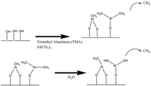
Among the different processes published in the literature, the synthesis of Al2O3 from trimethylaluminum (TMA) and water is one of the better known, and the self-limited growth of Al2O3 can be achieved in a wide range of temperature ranging from room temperature to more than 300 °C.[1]
During the TMA exposure, TMA dissociatively chemisorbs on the substrate surface and any remaining TMA is pumped out of the chamber. The dissociative chemisorption of TMA leaves a surface covered with AlCH3. The surface is then exposed to H2O vapor, which reacts with the surface –CH3 forming CH4 as a reaction byproduct and resulting on a hydroxylated Al2O3 surface.
Metal ALD
Metal ALD via elimination reactions most commonly occurs when metals functionalized with halogens (i.e. metal fluorides) are reacted with silicon precursors. Common metals deposited using fluorosilane elimination reactions are tungsten and molybdenum because the respective elimination reactions for these metals are highly exothermic[16] For Tungsten ALD, Si–H and W–F entities exist on the material's surface prior to the final purging process, and a linear deposition rate of W has been observed per each AB reactant cycle. Typical growth rates per cycle for Tungsten ALD are 4 to 7 Angstroms and typical reaction temperatures are 177 °C to 325 °C. Two surface reactions, as well as an overall ALD reaction for tungsten ALD, are presented below. A multitude of other metals can be deposited by ALD via the reactions below if their reaction sequences are based on fluorosilane elimination.
- Primary Reactions at Surface:
- WSiF2H* + WF6--> WWF5* + SiF3H (7)
- WF5* + Si2H6 --> WSiF2H* + SiF3H + 2H2 (8)
- Overall ALD Reaction:
- WF6 + Si2H6 --> W + 2SiF3H + 2H2 ∆H = -181kcal (9)
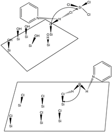
Catalytic SiO2 ALD
The use of catalysts is of paramount importance in delivering reliable methods of SiO2 ALD. Without catalysts, surface reactions leading to the formation of SiO2 are generally very slow and only occur at exceptionally high temperatures. Typical catalysts for SiO2 ALD include Lewis bases such as NH3 or pyridine and SiO2 ; ALD can also be initiated when these Lewis bases are coupled with other silicon precursors such as tetraethoxysilane (TEOS).[15] Hydrogen bonding is believed to occur between the Lewis base and the SiOH* surface species or between the H2O based reactant and the Lewis base. Oxygen becomes a stronger nucleophile when the Lewis base hydrogen bonds with the SiOH* surface species because the SiO-H bond is effectively weakened. As such, the electropositive Si atom in the SiCl4 reactant is more susceptible to nucleophilic attack. Similarly, hydrogen bonding between a Lewis base and an H2O reactant make the electronegative O in H2O a strong nucleophile that is able to attack the Si in an existing SiCl* surface species.[17] The use of a Lewis base catalyst is more or less a requirement for SiO2 ALD, as without a Lewis base catalyst, reaction temperatures must exceed 325 °C and pressures must exceed 103 torr. Generally, the most favorable temperature to perform SiO2 ALD is at 32 °C and a common deposition rate is 1.35 Angstroms per binary reaction sequence. Two surface reactions for SiO2 ALD, an overall reaction, and a schematic illustrating Lewis base catalysis in SiO2 ALD are provided below.
- Primary Reactions at Surface:
- SiOH* + SiCl4--> SiOSiCl3* + HCl (4)
- SiCl* + H2O --> SiOH* + HCl (5)
- Overall ALD Reaction:
- SiCl4 + 2H2O --> SiO2 + 4HCl (6)
| Type of ALD | Temperature range | Viable precursors | Reactants | Applications |
|---|---|---|---|---|
| Catalytic ALD | >32 °C with Lewis Base Catalyst[15] | Metal oxides (i.e. TiO2, ZrO2,SnO22)[15] | (Metal)Cl4, H2O[15] | High k-dielectric layers, protective layers, anti-reflective layers, etc.[15] |
| Al2O3 ALD | 30–300 °C | Al2O3, metal oxides[18] | (Metal)Cl4, H2O, Ti(OiPr)4, (Metal)(Et)2[15] | Dielectric layers, insulating layers, etc., Solar Cell surface passivations[18] |
| Metal ALD Using Thermal Chemistry | 175–400 °C[19] | Metal Fluorides, organometallics, catalytic metals[19] | M(C5H5)2, (CH3C5H4)M(CH3)3 ,Cu(thd)2, Pd(hfac)2, Ni(acac)2, H2[19] | Conductive pathways, catalytic surfaces, MOS devices[19] |
| ALD on polymers | 25–100 °C[15] | Common polymers (Polyethylene, PMMA, PP, PS, PVC, PVA, etc.)[15] | Al(CH3)3, H2O, M(CH3)3[15] | Polymer surface functionalization, creation of composites, diffusion barriers, etc.[15] |
| ALD on particles | Varies: 25–100 deg C for polymer particles, 100–400 deg C for metal/alloy particles[15] | BN, ZrO2, CNTs, polymer particles | Various gases: Fluidized bed reactors are used to allow coating of individual particles[15] | Deposition of protective and insulative coatings, optical and mechanical property modification, formation of composite structures, conductive mediums |
| Plasma or Radical-enhanced ALD for single element ALD materials | 20–800 °C[20][15] | Pure metals (i.e. Ta, Ti, Si, Ge, Ru, Pt), metal nitrides (i.e. TiN, TaN, etc.)[15] | Organometallics, MH2Cl2, tertbutylimidotris(diethylamido)tantalum (TBTDET), bis(ethylcyclopentadienyl)ruthenium), NH3[15] | DRAM structures, MOSFET and semiconductor devices, capacitors[21] |
| Plasma Enhanced ALD of Metal Oxides and Nitrides | 20–300 °C | Al2O3, SiO2, ZnOx, InOx, HfO2, SiNx, TaNx[22][23][24] | similar to thermal ALD |
Applications
ALD can be used for a great deal of applications. Some of the main fields that ALD is used for are microelectronics and biomedical applications. Details about these applications are outlined in the following sections.
Microelectronics applications
ALD is a useful process for the fabrication of microelectronics due to its ability to produce accurate thicknesses and uniform surfaces in addition to high quality film production using various different materials. In microelectronics, ALD is studied as a potential technique to deposit high-κ (high permittivity) gate oxides, high-κ memory capacitor dielectrics, ferroelectrics, and metals and nitrides for electrodes and interconnects. In high-κ gate oxides, where the control of ultra thin films is essential, ALD is only likely to come into wider use at the 45 nm technology. In metallizations, conformal films are required; currently it is expected that ALD will be used in mainstream production at the 65 nm node. In dynamic random access memories (DRAMs), the conformality requirements are even higher and ALD is the only method that can be used when feature sizes become smaller than 100 nm.[25] Several products that use ALD include magnetic recording heads, MOSFET gate stacks, DRAM capacitors, nonvolatile ferroelectric memories, and many others.
Gate oxides
Deposition of the high-κ oxides Al2O3, ZrO2, and HfO2 has been one of the most widely examined areas of ALD. The motivation for high-κ oxides comes from the problem of high tunneling current through the commonly used SiO2 gate dielectric in metal-oxide-semiconductor field-effect transistors (MOSFETs) when it is downscaled to a thickness of 1.0 nm and below. With the high-κ oxide, a thicker gate dielectric can be made for the required capacitance density, thus the tunneling current can be reduced through the structure.
Intel Corporation has reported using ALD to deposit high-κ gate dielectric for its 45 nm CMOS technology.[26]
Transition-metal nitrides
Transition-metal nitrides, such as TiN and TaN find potential use both as metal barriers and as gate metals. Metal barriers are used in modern Cu-based chips to avoid diffusion of Cu into the surrounding materials, such as insulators and the silicon substrate, and also, to prevent Cu contamination by elements diffusing from the insulators by surrounding every Cu interconnection with a layer of metal barriers. The metal barriers have strict demands: they should be pure; dense; conductive; conformal; thin; have good adhesion towards metals and insulators. The requirements concerning process technique can be fulfilled by ALD. The most studied ALD nitride is TiN which is deposited from TiCl4 and NH3.[27]
Metal films
Motivations of an interest in metal ALD are:
- Cu interconnects and W plugs, or at least Cu seed layers[28] for Cu electrodeposition and W seeds for W CVD,
- transition-metal nitrides (e.g. TiN, TaN, WN) for Cu interconnect barriers
- noble metals for ferroelectric random access memory (FRAM) and DRAM capacitor electrodes
- high- and low-work function metals for dual-gate MOSFETs.
Magnetic recording heads
Magnetic recording heads utilize electric fields to polarize particles and leave a magnetized pattern on a hard disk.[29] Al2O3 ALD is used to create uniform, thin layers of insulation.[30] By using ALD, it is possible to control the insulation thickness to a high level of accuracy. This allows for more accurate patterns of magnetized particles and thus higher quality recordings.
DRAM capacitors
Dynamic random-access memory (DRAM) capacitors are yet another application of ALD. An individual DRAM cell can store a single bit of data and consists of a single MOS transistor and a capacitor. Major efforts are being put into reducing the size of the capacitor which will effectively allow for greater memory density. In order to change the capacitor size without affecting the capacitance, different cell orientations are being used. Some of these include stacked or trench capacitors.[31] With the emergence of trench capacitors, the problem of fabricating these capacitors comes into play, especially as the size of semiconductors decreases. ALD allows trench features to be scaled to beyond 100 nm. The ability to deposit single layers of material allows for a great deal of control over the material. Except for some issues of incomplete film growth (largely due to insufficient amount or low temperature substrates), ALD provides an effective means of depositing thin films like dielectrics or barriers.[32]
Biomedical applications
Understanding and being able to specify the surface properties on biomedical devices is critical in the biomedical industry, especially regarding devices that are implanted in the body. A material interacts with the environment at its surface, so the surface properties largely direct the interactions of the material with its environment. Surface chemistry and surface topography affect protein adsorption, cellular interactions, and the immune response[33]
Some current uses in biomedical applications include creating flexible sensors, modifying nanoporous membranes, polymer ALD, and creating thin biocompatible coatings. ALD has been used to deposit TiO2 films to create optical waveguide sensors as diagnostic tools.[34] Also, ALD is beneficial in creating flexible sensing devices that can be used, for example, in the clothing of athletes to detect movement or heart rate. ALD is one possible manufacturing process for flexible organic field-effect transistors (OFETs) because it is a low-temperature deposition method.[35]
Nanoporous materials are emerging throughout the biomedical industry in drug delivery, implants, and tissue engineering. The benefit of using ALD to modify the surfaces of nanoporous materials is that, unlike many other methods, the saturation and self-limiting nature of the reactions means that even deeply embedded surfaces and interfaces are coated with a uniform film. Nanoporous surfaces can have their pore size reduced further in the ALD process because the conformal coating will completely coat the insides of the pores. This reduction in pore size may be advantageous in certain applications .[36]
Quality and quality control
The quality of an ALD process can be monitored using several different imaging techniques to make sure that the ALD process is occurring smoothly and producing a conformal layer over a surface. One option is cross-sectional SEM images or transmission electron microscopy (TEM) images, which allow for inspection at the micro and nano scale. High magnification of images is pertinent for assessing the quality of an ALD layer. XRR, or X-ray reflectivity, is a technique that measures thin-film properties including thickness, density, and surface roughness.[37] Another optical quality evaluation tool is spectroscopic ellipsometry (SE). Using SE in between the depositions of each layer added on by ALD provides information on the growth rate and material characteristics of the film can be assessed.[38]
Applying this analysis tool during the ALD process, sometimes referred to as in situ spectroscopic ellipsometry, allows for greater control over the growth rate of the films during the ALD process. This type of quality control occurs during the ALD process rather than assessing the films afterwards as in TEM imaging, or XRR. Additionally, Rutherford backscattering spectroscopy (RBS), X-Ray photoelectron spectroscopy (XPS), Auger electron spectroscopy (AES), and four-point probe (FPP) are some other techniques that can be used to provide quality control information with regards to thin films deposited by ALD.[38]
Advantages and limitations
Advantages
ALD provides a very controlled method to produce a film to an atomically specified thickness. Also, the growth of different multilayer structures is straightforward. Due to the sensitivity and precision of the equipment, it is very beneficial to those in the field of microelectronics and nanotechnology in producing small, but efficient semiconductors. ALD is typically run at lower temperatures along with a catalyst which is thermochemically favored. The lower temperature is beneficial when working with fragile substrates, such as biological samples. Some precursors that are thermally unstable still may be used so long as their decomposition rate is relatively slow.[15]
Disadvantages
High purity of the substrates is very important, and as such, high costs will ensue (Stanford). Although this cost may not be much relative to the cost of the equipment needed, one may need to run several trials before finding conditions that favor their desired product. Once the layer has been made and the process is complete, there may be a requirement of needing to remove excess precursors from the final product. In some final products there are less than one percent of impurities present.[39]
Economic viability
Atomic layer deposition instruments can range anywhere from $200,000 to $800,000 based on the quality and efficiency of the instrument. There is no set cost for running a cycle of these instruments; the cost varies depending on the quality and purity of the substrates used, as well as the temperature and time of machine operation. Some substrates are less available than others and require special conditions, as some are very sensitive to oxygen and may then increase the rate of decomposition. Multicomponent oxides and certain metals traditionally needed in the microelectronics industry are generally not cost efficient.[40]
Reaction time
The process of ALD is very slow and this is known to be its major limitation. For example, Al2O3 is deposited at a rate of 0.11 nm per cycle,[1] which can correspond to an average deposition rate of 100–300 nm per hour, depending on cycle duration and pumping speed. ALD is typically used to produce substrates for microelectronics and nanotechnology, and therefore, thick atomic layers are not needed. Many substrates cannot be used because of their fragility or impurity. Impurities are typically found on the 0.1-1% atomic level because of some of the carrier gases are known to leave residue and are also sensitive to oxygen.[39]
Chemical limitations
Precursors must be volatile, but not subject to decomposition, as most precursors are very sensitive to oxygen/air, thus causing a limitation on the substrates that may be used. Some biological substrates are very sensitive to heat and may have fast decomposition rates that are not favored and yield larger impurity levels. There are a multitude of thin-film substrate materials available, but the important substrates needed for use in microelectronics can be hard to obtain and may be very expensive.[39]
References
- 1 2 3 4 5 6 Puurunen, Riikka L. (15 June 2005). "Surface chemistry of atomic layer deposition: A case study for the trimethylaluminum/water process". Journal of Applied Physics. 97 (12): 121301. doi:10.1063/1.1940727. ISSN 0021-8979.
- 1 2 Miikkulainen, Ville; Leskelä, Markku; Ritala, Mikko; Puurunen, Riikka L. (14 January 2013). "Crystallinity of inorganic films grown by atomic layer deposition: Overview and general trends". Journal of Applied Physics. 113 (2): 021301. doi:10.1063/1.4757907. ISSN 0021-8979.
- 1 2 Ahvenniemi, Esko; Akbashev, Andrew R.; Ali, Saima; Bechelany, Mikhael; Berdova, Maria; Boyadjiev, Stefan; Cameron, David C.; Chen, Rong; Chubarov, Mikhail (16 December 2016). "Review Article: Recommended reading list of early publications on atomic layer deposition—Outcome of the "Virtual Project on the History of ALD"". Journal of Vacuum Science & Technology A: Vacuum, Surfaces, and Films. 35 (1): 010801. doi:10.1116/1.4971389. ISSN 0734-2101.
- ↑ Virtual project on the history of ALD (VPHA) website http://www.vph-ald.com
- 1 2 3 4 5 6 7 8 9 10 11 12 13 Puurunen, Riikka L. (1 December 2014). "A Short History of Atomic Layer Deposition: Tuomo Suntola's Atomic Layer Epitaxy". Chemical Vapor Deposition. 20 (10-11–12): 332–344. doi:10.1002/cvde.201402012. ISSN 1521-3862.
- 1 2 3 4 5 6 7 8 Malygin, Anatolii A.; Drozd, Victor E.; Malkov, Anatolii A.; Smirnov, Vladimir M. (1 December 2015). "From V. B. Aleskovskii's "Framework" Hypothesis to the Method of Molecular Layering/Atomic Layer Deposition". Chemical Vapor Deposition. 21 (10-11–12): 216–240. doi:10.1002/cvde.201502013. ISSN 1521-3862.
- ↑ V. B. Aleskovskii, Zh. Prikl. Khim. 47, 2145 (1974); [J. Appl. Chem. USSR. 47, 2207, (1974)].
- 1 2 3 T. Suntola, J. Antson, U.S. Patent 4,058,430, 1977
- ↑ T. Suntola, A. Pakkala, S. Lindfors, U.S. Patent 4,389,97, 1983
- ↑ "2018 Millennium Technology Prize for Tuomo Suntola – Finnish physicist's innovation enables manufacture and development of information technology products" (Press release). Technology Academy Finland. 2018-05-22. Retrieved 2018-05-22.
- ↑ Parsons, Gregory N.; Elam, Jeffrey W.; George, Steven M.; Haukka, Suvi; Jeon, Hyeongtag; Kessels, W. M. M. (Erwin); Leskelä, Markku; Poodt, Paul; Ritala, Mikko (1 September 2013). "History of atomic layer deposition and its relationship with the American VacuumSociety". Journal of Vacuum Science & Technology A. 31 (5): 050818. doi:10.1116/1.4816548. ISSN 0734-2101.
- ↑ "How Atomic Layer Deposition Works" Applied Materials. https://www.youtube.com/watch?v=KOEsgZU1sts
- ↑ Hans-Jurgen Butt; Karlheinz Graf; Michael Kappl (2013). Physics and Chemistry of Interfaces (Third, Revised ed.). ISBN 978-3-527-41216-7.
- ↑ "2.3 Adsorption Kinetics - The Rate of Adsorption". www.chem.qmul.ac.uk.
- 1 2 3 4 5 6 7 8 9 10 11 12 13 14 15 16 17 George, S.M. (2010). "Atomic Layer Deposition: An Overview". Chem. Rev. 110: 111–131. doi:10.1021/cr900056b.
- ↑ Juppo, M. "Atomic Layer Deposition of Metal and Transition Metal Nitride Thin Films and In-Situ Mass Spectrometry Studies" University of Helsinki Department of Chemistry, Laboratory of Inorganic Chemistry. Dec. 2001.
- ↑ Brown, S.; Howe, J.Y.; Ma, Z.; Et (2008). "Surface Modification of Au/TiO2 Catalysts by SiO2 via Atomic Layer Deposition". The Journal of Physical Chemistry C. 112 (25): 9448–9457. doi:10.1021/jp801484h.
- 1 2 Florian Werner; Walter Stals; Roger Gortzen; Boris Veith; Rolf Brendel; Jan Schmidt (2011). "High-rate atomic layer deposition of Al2O3 for the surface passivation of Si solar cells". Energy Procedia. 8: 1301–306.
- 1 2 3 4 H. Kim (2003). "Atomic layer deposition of metal and nitride thin films: Current research efforts and applications for semiconductor device processing". Journal of Vacuum Science and Technology. 21 (6): 2231. doi:10.1116/1.1622676.
- ↑ Mackus, Adriaan J. M.; Garcia-Alonso, Diana; Knoops, Harm C. M.; Bol, Ageeth A.; Kessels, Wilhelmus M. M. (14 May 2013). "Room-Temperature Atomic Layer Deposition of Platinum". Chemistry of Materials. 25 (9): 1769–1774. doi:10.1021/cm400274n.
- ↑ "Fundamental Vacuum Beam Studies of Radical Enhanced Atomic Layer Chemical Vapor Deposition (REAL-CVD) of TiN" Dr. Frank Greer, Dr. D. Fraser, Dr. J.W. Coburn, and Professor David B. Graves, NCCAVS, 12 December 2002. "Archived copy" (PDF). Archived from the original (PDF) on 14 July 2014. Retrieved 7 June 2014.
- ↑ Potts, S.E.; Kessels, W.M.M. (December 2013). "Energy-enhanced atomic layer deposition for more process and precursor versatility". Coordination Chemistry Reviews. 257 (23–24): 3254–3270. doi:10.1016/j.ccr.2013.06.015.
- ↑ Knoops, Harm C. M.; Braeken, Eline M. J.; de Peuter, Koen; Potts, Stephen E.; Haukka, Suvi; Pore, Viljami; Kessels, Wilhelmus M. M. (9 September 2015). "Atomic Layer Deposition of Silicon Nitride from Bis( -butylamino)silane and N Plasma". ACS Applied Materials & Interfaces. 7 (35): 19857–19862. doi:10.1021/acsami.5b06833.
- ↑ Langereis, E.; Knoops, H. C. M.; Mackus, A. J. M.; Roozeboom, F.; van de Sanden, M. C. M.; Kessels, W. M. M. (15 October 2007). "Synthesis and characterization of low-resistivity TaNx films by remote plasma atomic layer deposition". Journal of Applied Physics. 102 (8): 083517. doi:10.1063/1.2798598.
- ↑ A. Ahnd, Semicond. Int. 26, 46–51, 2003.
- ↑ "A 45nm Logic Technology with High-k+Metal Gate Transistors, Strained Silicon, 9 Cu Interconnect Layers, 193nm Dry Patterning, and 100% Pb-free Packaging" (PDF). 18 February 2008. Archived from the original (PDF) on 18 February 2008.
- ↑ K.E. Elers et al.,Chem. Vap. Deposition 4,149, 2002
- ↑ Waechtler, T.; et al. (2011). "ALD-grown seed layers for electrochemical copper deposition integrated with different diffusion barrier systems". Microelectron. Eng. 88: 684–689. doi:10.1016/j.mee.2010.07.004.
- ↑ Archived 11 July 2010 at the Wayback Machine.
- ↑ "JJ-Net Group Oy". www.miics.net.
- ↑ http://smithsonianchips.si.edu/ice/cd/MEMORY97/SEC07.PDF
- ↑ Archived 8 September 2005 at the Wayback Machine.
- ↑ Chen, Hong; Yuan, Lin; Song, Wei; Wu, Shongkui; Li, Dan (2008). "Biocompatible Polymer Materials: Role of Protein-surface Interactions". Progress in Polymer Science. 33 (11): 1059–1087. doi:10.1016/j.progpolymsci.2008.07.006.
- ↑ Purniawan, A.; French, P.J.; Pandraud, G.; Sarro, P.M. (2010). "TiO2 ALD nanolayer as evanescent waveguide for biomedical sensor applications". Procedia Engineering. 5: 1131–1135. doi:10.1016/j.proeng.2010.09.310.
- ↑ Pang, Changhyun; Lee, Chanseok; Suh, Kahp-Yang (2013). "Recent Advances in Flexible Sensors for Wearable and Implantable Devices". Applied Polymer Science. 130: 1429–1441. doi:10.1002/app.39461.
- ↑ Hill, Univ. of North Carolina at Chapel; J Zhang; C.M Shin; M. J Pellin; S. D Gittard; S. P. Curtiss; L. A Adiga; S.J Lin; Y.Y Su; J. W Elam; R. J Narayan; National Yang-Ming Univ; C.C Shih; Taipei Medical Univ. (2008). "Nanoporous Materials for Biomedical Devices". Biological Materials Science. 60 (3): 26–32.
- ↑ Yasaka, Miho (2010). "X-ray thin-film measurement techniques". The Rigaku Journal. 26 (2): 1–9.
- 1 2 E Langereis; S B S Heil; H C M Knoops; W Keuning; M C M van de Sanden; W M M Kessels (2009). "In situ spectroscopic ellipsometry as a versatile tool for studying atomic layer deposition". Journal of Physics D: Applied Physics. 42: 1–19. doi:10.1088/0022-3727/42/7/073001.
- 1 2 3 http://files.instrument.com.cn/FilesCenter/20060216/18273.pdf
- ↑ "Molecular Beam Epitaxy & Atomic Layer Deposition Systems - SVT Associates". www.svta.com.