350 nanometer
| Semiconductor manufacturing processes |
|---|
 |
|
Half-nodes |
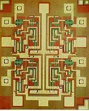
The 350 nanometer (350 nm) process refers to the level of semiconductor process technology that was reached in the 1995–1996 timeframe, by most leading semiconductor companies, like Intel and IBM.
Products featuring 350 nm manufacturing process
- MTI VR4300i (1995), used in the Nintendo 64 game console.
- Intel Pentium (P54CS, 1995), Pentium Pro (1995) and initial Pentium II CPUs (Klamath, 1997).
- AMD K5 (1996) and original AMD K6 (Model 6, 1997) CPUs.
- МЦСТ-R150 (2001).
- Parallax Propeller (2006), 8 core microcontroller[1].
References
- ↑ "Propeller I semiconductor process technology? Is it 350nm or 180nm? - Parallax Forums". Forums.parallax.com. Retrieved 2015-09-13.
| Preceded by 600 nm |
CMOS manufacturing processes | Succeeded by 250 nm |
This article is issued from
Wikipedia.
The text is licensed under Creative Commons - Attribution - Sharealike.
Additional terms may apply for the media files.